Explore production-grade SMD board assemblies engineered to IPC-A-610 Class 3 specifications across aerospace, medical instrumentation, smart energy monitoring, and heavy industrial automation.
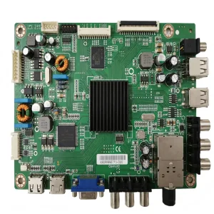

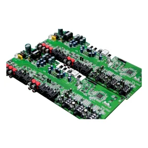

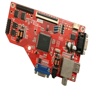
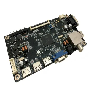
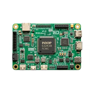
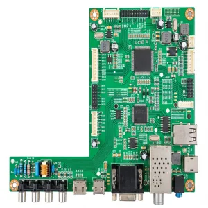
Surface Mount Device (SMD) assembly has evolved from basic component placement into an ultra-dense, multi-physics discipline demanding nanometer solder alignment, thermal balance management, and closed-loop optical intelligence.
Today's electronics architectures mandate 01005 (0402 metric) and emerging 008004 discrete chip components alongside 0.3mm pitch fine-ball grid arrays (BGA) and Wafer-Level Chip-Scale Packaging (WLCSP). OEM manufacturers must deploy high-speed dynamic vision centering with mounting accuracies exceeding ±15 microns at 3-sigma limits.
Lead-free alloys (SAC305, SAC0307, and low-temp bismuth formulations) require strictly controlled reflow ovens with 10 to 12 heating zones and integrated nitrogen (N2) atmospheres. Limiting delta-T variation across hybrid heavy-copper and flexible circuit boards prevents cold joints, tombstoning, and void formation under QFN thermal pads.
More than 70% of SMD assembly defects originate during the stencil printing phase. Industrial SMT lines integrate closed-loop 3D Solder Paste Inspection (SPI) systems that communicate directly with laser-guided stencil printers, automatically offsetting squeegee pressure, speed, and cleaning cycles upon detecting micro-volume deviations.
Procurement directors and Chief Technology Officers across North America, Europe, and Asia-Pacific are transitioning from fragmented transactional contracting to comprehensive Turnkey EMS partnerships that actively mitigate market volatility.
Modern hardware life cycles are frequently derailed by semiconductor supply bottlenecks, End-of-Life (EOL) notices, and unpredictable allocation cycles. High-tier OEM SMD factories leverage direct API integrations with franchised distributors (including Arrow, Avnet, Digi-Key, Mouser, and Farnell) combined with localized spot-buy verification hubs.
By conducting automated Bill of Materials (BOM) health checks at the quotation stage, engineering teams can propose verified Second-Source Alternatives and Pin-to-Pin equivalents before copper laminates ever enter the fabrication queue, ensuring production continuity without sacrificing functional compliance.
Purchasing bare PCBs from one vendor, loose SMD reels from brokers, and contracting consignment assembly from an offshore workshop introduces hidden logistics friction, customs delays, and unresolved blame allocation when yields drop. A single turnkey manufacturer assumes unified responsibility across:
Bare board fabrication, IPC Class 3 solderability, moisture barrier packaging, conformal coating, functional in-circuit testing (ICT), firmware flash programming, and system box build. This consolidation reduces internal project management overhead by up to 40% while accelerating time-to-market.
True OEM manufacturing excellence is established long before the SMT feeder indexer activates. STHL's engineering review deploys exhaustive DFM/DFA checks across every project: analyzing solder mask dam clearances, copper balance across internal signal planes to avert thermal board bow and twist, fiducial marker placement for optical vision recognition, and pad geometry optimization according to IPC-7351 guidelines. Identifying stencil aperture aspect ratio mismatches or shadowing effects during DFM prevents costly production re-spins and optimizes downstream assembly throughput.
Request Engineering Capability & SMT Guideline CatalogLocated in the heart of the Greater Bay Area, Shenzhen represents the world's most concentrated microelectronics supply ecosystem, combining sub-kilometer component sourcing velocity with cutting-edge smart manufacturing automation.
Every peripheral requirement—from customized metal enclosures, molded plastic tooling, and specialized silicone gaskets to rare passive component reels—can be acquired within an hour from Shenzhen's specialized industrial districts.
Every individual reel, paste pot, and bare board lot is serialized via 2D DataMatrix codes. Our Manufacturing Execution System (MES) links operator ID, placement feeder slot, solder batch, and reflow log to each finished board.
High-efficiency dual-lane pick-and-place lines running Yamaha and Panasonic modular mounters allow zero-downtime reel changeovers. Smart automated optical inspection (AOI) rapidly distinguishes true anomalies from false calls.
Adherence to IATF 16949 (automotive), ISO 13485 (medical), ISO 9001, and ISO 14001 frameworks guarantees that low-cost production scale never compromises baseline reliability, process capability (Cpk), or environmental compliance.
SMD board assemblies operate within extreme operating environments. Our manufacturing lines adapt soldering alloys, potting, conformal coatings, and stress-testing protocols to each specific industrial discipline.
VHF Omnidirectional Range (VOR) receiver assemblies (such as the China VOR Receiver PCBA Assembly) operate in high-vibration aviation environments subject to extreme temperature swings. Assembly involves impedance-controlled RF circuit traces, precision electromagnetic shielding (EMI cans) soldered with micro-gaps, and thermal cyclic burn-in to guarantee signal integrity across high-frequency navigation spectrums.
Solar energy arrays and micro-inverter power conditioning units demand assemblies like our OEM Photovoltaic Power Generation Monitoring System PCBA. These boards incorporate thick-copper power layers, high-creepage isolation barriers, and automated conformal coating to withstand high UV exposure, ambient humidity, and sustained elevated thermal cycling without dielectric breakdown.
From wearable physiological tracking apparatus to ultra-reliable pacemaker telemetry PCBA assemblies, medical surface-mount manufacturing demands IPC Class 3 compliance, cleanroom ESD-controlled assembly, 100% automated 3D X-Ray Inspection (AXI) of concealed BGA ball interconnects, and absolute material traceability with biocompatibility safeguards.
Modern DIN Rail and DC-DC power supply boards utilize low-RDS(on) GaN and SiC surface-mount power transistors that dissipate extreme heat across compact areas. STHL employs metal-core printed boards (MCPCB), thick thermal vias, vacuum reflow soldering to virtually eliminate solder joint voids, and automated high-potential (Hi-Pot) safety testing.
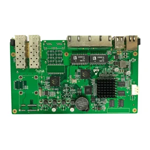
Next-generation FTTH networks rely on high-speed OLT assemblies featuring high-layer-count HDI boards (up to 32 layers) with blind and buried microvias. Precise impedance matching, ultra-low insertion loss dielectric substrates (e.g., Rogers, Megtron), and zero-stress component placement prevent signal attenuation in gigabit optical transceivers.
Combustible and hazardous gas monitoring instruments require intrinsically safe circuit designs. SMT placement mandates micro-pitch sensor interfaces, potting encapsulation for explosive atmospheres, and strict ionic contamination cleaning cycles conforming to IPC-CH-65B and ROSE test benchmarks.
At STHL, quality is verified scientifically at each manufacturing station. Statistical Process Control (SPC) and automated testing equipment validate electrical, structural, and environmental compliance at every gate.
Equipped with multi-directional Moire projection sensors, our dual 3D AOI machines inspect both pre- and post-reflow boards. The system accurately measures solder fillet height, detects bridge shorts, tombstones, lifted leads, polarity inversions, and component billboarding at sub-micron resolutions.
For ball grid arrays (BGA), Quad Flat No-leads (QFN), and leadless chip carriers (LCC) where solder joints are hidden beneath component bodies, high-resolution transmission 3D AXI inspects solder ball diameter, coplanarity, circularity, bridging, and calculates void percentages against IPC standards.
Custom bed-of-nails fixtures and flying probe testers perform comprehensive opens/shorts and component value verification. Dedicated functional test lines simulate real-world operational environments, measuring RF outputs, digital bus communication (CAN, RS-485, I2C, SPI), and loaded voltages.
Boards destined for harsh automotive, maritime, or outdoor photovoltaic deployments undergo thermal shock (-40°C to +125°C), high-temperature extended burn-in under power, and multi-axis vibration testing to accelerate infant mortality failures before shipment.
Resistivity of Solvent Extract (ROSE) testing verifies that post-soldering residue meets clean standards (<1.56 µg/cm² NaCl equivalent), preventing electrochemical migration, dendritic growth, and leakage currents in high-humidity deployments.
Robotic selective spray valves deposit uniform layers of acrylic, silicone, or polyurethane coatings. UV dye verification ensures pinhole-free coverage across sensitive circuit nodes while preserving test points, connectors, and switch contacts.
In-depth technical answers addressing the critical parameters global engineers and procurement managers evaluate when vetting PCB assembly manufacturers in China.
Our automated high-speed Panasonic and Yamaha SMT lines place down to 01005 (0402 metric) passives and 0.3mm pitch micro-BGAs and WLCSP devices. For micro-pitch components, we deploy electroformed stencils, nano-coatings, and Type 4 / Type 5 fine-grain solder pastes with 3D SPI verification to prevent bridge bridging or incomplete wet-out.
We enforce a strict Anti-Counterfeit Prevention Policy adhering to AS5553 and AS6081 guidelines. Sourcing is restricted to original component manufacturers (OCM) and authorized franchised distributors. For spot-market purchases, incoming components undergo decapsulation, microscopic die inspection, XRF elemental composition analysis, and pin solderability testing in our QA laboratory.
We execute legally binding Non-Disclosure Agreements (NDAs) prior to file submission. Engineering Gerber datasets, schematics, and firmware files are stored on isolated, encrypted servers with strict permission controls. IC programming operations are executed using locked hex files inside secure programming workstations with automated station logging.
Quick-turn PCBA prototypes can be assembled and shipped within 24 to 72 hours following component kit verification and bare PCB fabrication. Standard turnkey production runs typically take 2 to 4 weeks, depending primarily on component procurement lead times. Fast-track component reservation programs are available for recurring work orders.
To provide a detailed DFM evaluation and comprehensive quote, we require: (1) Gerber files in RS-274X or ODB++ format; (2) Bill of Materials (BOM) with manufacturer part numbers (MPN), descriptions, and reference designators; (3) Pick-and-Place Centroid (.xy) coordinate file; (4) Fabrication and Assembly drawings; and (5) Functional testing instructions.
Yes. Our Shenzhen facility operates 7 high-speed SMT lines, 2 selective soldering and lead-free wave soldering DIP/THT lines, dedicated manual soldering work-cells for sensitive components, along with 4 box build assembly and mechanical integration lines. We support rigid FR-4, flex, rigid-flex, and metal-core substrates under one unified quality system.
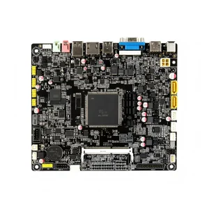
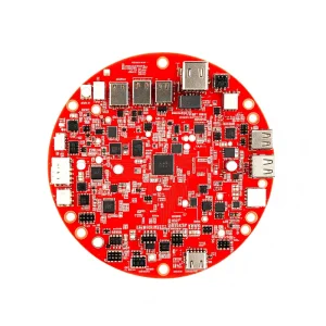
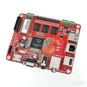
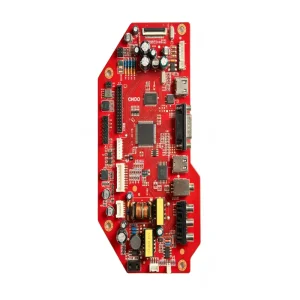
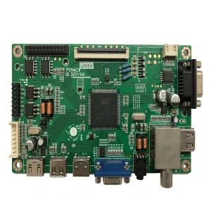
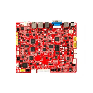
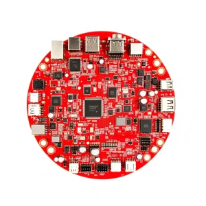
Demonstrated manufacturing capability across switching regulators, intelligent building automation, optical networking terminals, and high-density industrial control assemblies.
Send your Gerber files, BOM, and assembly drawings today. Our senior application engineers will complete an in-depth DFM report and transparent quotation within 24 hours.
