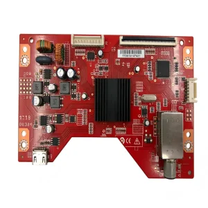
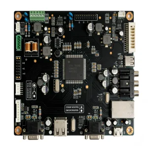
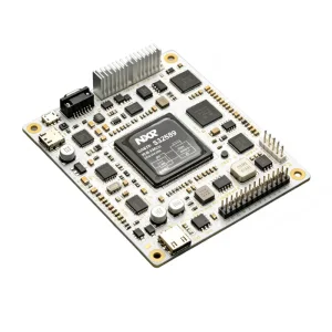
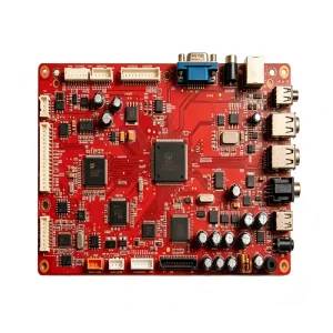
Engineered on ultra-fast, multi-zone automated SMD lines. Explore calibrated manufacturing runs for industrial, computing, and high-lumen optical integrations.
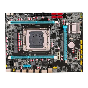

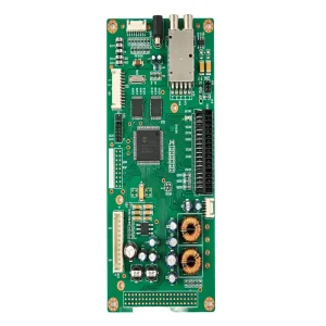
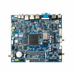
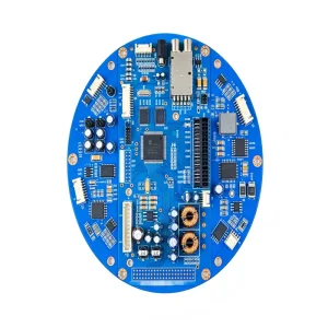
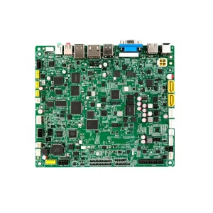
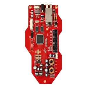
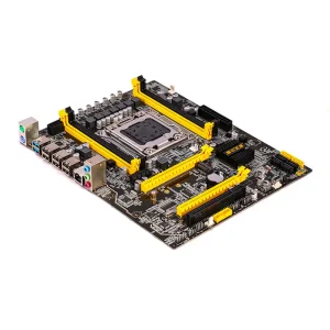
The electronics manufacturing services (EMS) sector has transitioned beyond traditional pick-and-place throughput. Modern high-reliability requirements demand AI-driven statistical process control, nanometer-level alignment, and end-to-end MES integration.
In the contemporary hardware manufacturing paradigm, modern Surface Mount Technology (SMT) and Surface Mount Device (SMD) production lines are no longer mere electromechanical conveyor systems. They represent high-density cyber-physical nodes within a digitalized supply chain. With the exponential growth of 5G infrastructure, electric vehicle (EV) powertrain ECUs, AI edge-computing accelerators, and implantable medical robotics, original equipment manufacturers (OEMs) face unprecedented engineering challenges: reducing real estate footprints down to 01005 (0402 metric) and 03015 micro-passives while simultaneously driving defect escape rates to zero parts-per-million (PPM).
Historically, contract electronics assembly evaluated factory capacity by simple Component-Per-Hour (CPH) ratings. Today, international procurement directors and Principal Quality Engineers realize raw CPH is a vanity metric if not backed by first-pass yield (FPY) integrity. The real technological battlefield centers on closed-loop feedback systems between 3D Solder Paste Inspection (SPI) machines and automatic solder paste stencil printers, continuous thermal profiling across 10-to-12 heating zones under controlled nitrogen atmospheres, and deterministic defect elimination prior to final conformal coating or box-build operations.
Deploying optical centering algorithms capable of resolving 0.3mm pitch Ball Grid Arrays (BGA), micro-CSPs, and Quad Flat No-Lead (QFN) components with zero coplanarity deviation.
Automated squeegee pressure modulation paired with real-time SPI communication, dynamically adjusting stencil alignment offsets before bridge defects or voids manifest.
Integrating sub-5mbar vacuum degassing modules within the liquidus phase to suppress solder void ratios beneath critical power semiconductor dies to under 8%.
A rigorous inspection of every critical station on an enterprise-class OEM surface mount assembly line, highlighting precision parameters, inspection gates, and quality verification standards.
| SMD Line Stage | Core Equipment & Mechanisms | Process Control Parameters | Acceptance Benchmark (IPC-A-610G) |
|---|---|---|---|
| 1. Laser Stencil Printing | Fully Automated High-Precision Printers with Enclosed ProFlow Heads | Repeatability: ±10 μm; Squeegee speed: 20-150 mm/s; Constant paste height | Volume deposition accuracy: 100% ±15%; Zero aperture bridging |
| 2. 3D Solder Paste Inspection (SPI) | Moiré Phase-Shift Optical Profilometry with Dual Digital Cameras | Height resolution: 0.1 μm; Area, volume, offset, bridging & coplanarity | Instant warning at >3 consecutive deviations; auto-feed back to printer |
| 3. High-Speed Modular Placement | Multi-Gantry Linear Motor Mounters (Fuji / Yamaha / Panasonic) | Component range: 01005 to 74×74mm; Placement speed: up to 90,000 CPH | Cpk ≥ 1.67; Theta rotation accuracy ±0.03°; Zero missing parts |
| 4. Pre-Reflow Automated Optical Inspection | Multi-Angle Color Structured Light Inspection Engines | Verifies component presence, orientation, polarity mark, and positional shift | False alarm rate < 50 PPM; Intercepts 99.8% of placement inaccuracies |
| 5. Nitrogen Convection Reflow | 10-12 Zone Forced Convection Ovens with O2 analyzer (<500 PPM O2) | Peak temp control: 235-245°C (SAC305); TAL: 60-90s; Max ramp rate: 2.5°C/s | Delta T across large thermal mass boards ≤ 2.5°C; Clean intermetallic layer |
| 6. Post-Reflow 3D AOI & 3D AXI | High-Definition 12-Megapixel Cameras + Oblique Angle X-Ray Tomography | Solder fillet curvature, tombstoning, wetting angle; BGA voiding & HIP defects | Class 3 IPC standard; BGA voids < 15% aggregate, < 8% single biggest void |
In high-reliability OEM assembly, joint failure typically originates at the microscopic metallurgical boundary. During the liquidus phase in our convection reflow tunnels, lead-free alloys (such as SAC305: 96.5% Sn, 3.0% Ag, 0.5% Cu) react with copper substrate metallization to generate Cu6Sn5 intermetallic compound (IMC) scallops. If thermal input is uncalibrated, excessive dwell times trigger brittle Cu3Sn phase thickening, degrading vibration and thermal shock resilience. STHL's engineering framework deploys 9-channel real-time thermal profilers to enforce continuous liquidus cooling gradients between 2.0°C/s and 4.0°C/s, ensuring thin, ductile IMC layers (< 2.5 μm) that comply rigorously with automotive IATF 16949 and medical ISO 13485 standards.
Design for Excellence (DFM/DFA) Notice: Optimal SMD line yield begins at the layout level. Stencil aperture ratios (Area Ratio ≥ 0.66, Aspect Ratio ≥ 1.5) must be cross-matched against board copper weight, thermal relief vias, and component termination geometries. STHL engineers perform automated DFM evaluations on all Gerber, ODB++, and BOM packages before stencil laser-cutting commences.
How procurement managers and VP of Engineering eliminate lead-time volatility, component obsolescence, and counterfeit infiltration through certified OEM electronic contract manufacturing.
Our centralized procurement network partners with factory-direct franchise distributors (Arrow, Avnet, Digi-Key, Mouser) alongside verified Tier-1 semiconductor lines. In-house verification features decapsulation testing, XRF elemental composition analysis, and solderability confirmation under IDEA-STD-1010 standards to guarantee 100% genuine components.
Supply chain shocks can halt an entire SMT line due to a single missing passive or MCU. Our 50+ engineering personnel cross-reference active BOMs against silicon silicon roadmaps, preemptively proposing second-source Pin-to-Pin (P2P) functional equivalents without necessitating schematic redesigns or re-certification overheads.
Eliminating minimum order quantities (Zero MOQ), STHL accommodates quick-turn prototype evaluation runs (24-to-48 hours) alongside mass industrial deployments. Fast-changeover intelligent feeders and offline setup verification systems shorten product line changeover times to under 15 minutes, maintaining high overall equipment effectiveness (OEE).
From harsh-environment automotive under-the-hood microcontrollers to high-reliability Class III surgical guidance platforms, STHL customizes SMT profile recipes and conformal protective chemistries.
Certified under IATF 16949:2016, our SMT lines run specialized high-Tg FR-4 and ceramic substrates for Transmission Control Units (TCU) and On-Board Chargers (OBC). With Automated X-ray Inspection (AXI) analyzing multi-layer solder voids and selective conformal coating shielding against moisture and thermal fatigue, our assemblies guarantee 15-year operational lifespans under automotive shock and vibration.
Under ISO 13485 oversight, PCBA builds for surgical navigation systems and diagnostic vital-sign monitors undergo Class 3 medical traceability. Every individual SMT component lot, reel serial number, and reflow profile is permanently logged into our Manufacturing Execution System (MES), preventing unverified component substitutions and ensuring regulatory compliance with FDA and CE-MDR requirements.
Solar inverters and grid-tied power electronics demand heavy-copper PCBs (3oz to 6oz) to sustain large thermal currents. Our automated DIP wave soldering and selective soldering lines work in direct synchronization with surface-mount pick-and-place systems, providing optimal inter-metallic bonding on heavy-pin transformers, power MOSFETs, and high-voltage DC-link capacitors.
From aluminum core PCBs (MCPCB) to ultra-long flexible LED strip arrays, our dedicated surface-mount lines are equipped with long-board feed conveyors (handling lengths up to 1.5 meters without splicing). Optical color-bin matching and precise thermal interface material (TIM) dispensing deliver optimal lumen maintenance and heat dissipation.
Transparent process records from raw silicon receipt to outgoing carton dispatch. We ensure end-to-end verification and accountability.
Enterprise sourcing leaders require more than verbal assurances; they demand verifiable digital audit trails. STHL operates an integrated Enterprise Resource Planning (ERP) and Manufacturing Execution System (MES) architecture that binds every serialized printed circuit board assembly (PCBA) to an indelible digital twin.
Upon arrival in our climate-controlled, ESD-protected warehouse (ANSI/ESD S20.20 compliant), all electronic component reels receive a unique 2D DataMatrix code detailing manufacturer lot code, date code, distributor batch ID, and internal receiving QC test logs. When feeders are mounted onto the SMD pick-and-place gantries, automated barcode scanners cross-check part placement data against the active CAD centroid coordinate file. If an operator mounts an incorrect reel or an expired moisture-sensitive device (MSD - J-STD-033C), the entire production line locks down instantly, preventing assembly escapes at the source.
Workmanship certifications covering solder joint fillet dimensions, barrel fill percentages on through-hole pins (>75%), and allowable coplanarity clearances on fine-pitch components.
Statistical Process Control (SPC) deployed at critical inspection nodes. CPK / PPK evaluations maintained ≥ 1.67, alongside comprehensive Failure Mode and Effects Analysis (FMEA) workflows.
Risk mitigation matrices, validation protocols (IQ/OQ/PQ) for all software and production tooling, and stringent hygiene/particulate controls in assembly rooms.
Zero hazardous substance declaration. Fully compliant with EU Directive 2015/863, SVHC screening, and Dodd-Frank Act Section 1502 transparent mineral supply chain tracking.
How cutting-edge surface-mount advancements are redefining density, thermal dissipation, and autonomous manufacturing intelligence for the next decade of electronic hardware.
The electronic hardware industry is approaching the fundamental physical boundaries of standard silicon packaging. Over the next five years, contract manufacturers must navigate tectonic shifts in materials science, automated inspection algorithms, and advanced substrate assembly techniques.
Transitioning from traditional rule-based AOI algorithms to deep neural networks trained on millions of solder meniscus images. Machine-learning models classify marginal wetting, micro-bridging, and void distributions in real-time, eliminating human false calls while detecting hairline solder cracks that conventional optics miss.
With high-speed digital designs demanding minimal parasitic inductance, discrete passives and thin bare dies are increasingly embedded directly inside inner PCB laminate core layers. STHL's engineering roadmap incorporates specialized cavity dispensing, planar solder deposition, and laser Z-axis placement tools to support this architectural transition.
To reduce thermal stress on ultra-thin OLED flex circuits and cut carbon consumption during reflow, STHL is expanding its validation of Bismuth-doped Low-Temperature Solders (LTS) melting between 138°C and 170°C. This technical milestone minimizes PCB dynamic warpage by over 40% while slashing factory carbon footprints.
In-depth responses to critical questions surrounding SMD line capabilities, quality tolerances, testing coverage, and production scalability.
Manufactured across our 7 automated SMT lines. Explore specialized builds featuring rigorous traceability, vacuum reflow soldering, and IPC Class 3 quality controls.