
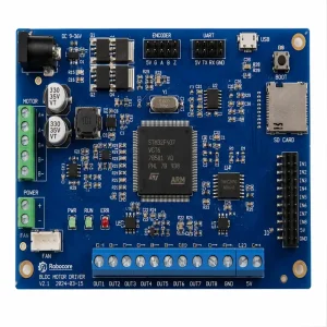
Turnkey production builds utilizing multi-zone reflow profiling, 3D SPI paste validation, and continuous component placement verification.
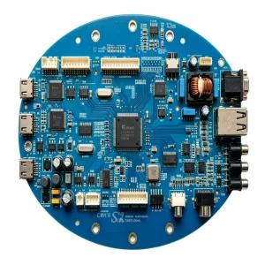
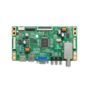
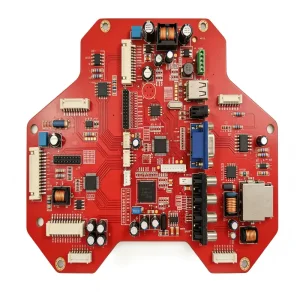


How the worldwide demand for miniaturization, edge computing, and extreme environmental resilience is rewriting the standards of Surface Mount Technology factories.
Global electronics demand has accelerated the adoption of ultra-dense passives (01005 and 0201 metric footprints) alongside high-pin-count CSP (Chip-Scale Packaging) and micro-BGAs with ball pitches collapsing below 0.35 mm.
Higher thermal dissipation from automotive power trains and industrial high-voltage drivers necessitates automated vacuum reflow soldering, eliminating internal voiding ratios down to less than 5% within power packages.
International procurement frameworks (IATF 16949, ISO 13485) mandate continuous data telemetry from Solder Paste Inspection (SPI), automated optical checks (AOI), and in-line X-ray analysis straight into MES platforms.
Combining dense geographical clustering, automated line flexibility, and round-the-clock engineering agility to drastically shorten Time-to-Market.
Located in Shenzhen's Bao'an electronics cluster, tier-1 active components, passive reels, and raw laminate substructures are accessible within hours, eliminating standard 4-week transit buffers common in Western or remote facilities.
Our 50+ on-site engineers perform deep design-for-manufacturing analyses prior to tooling. We identify pad geometry mismatches, thermal shadow hazards, and supply-risk components, proposing viable drops-in without design stalls.
From NPI (New Product Introduction) proof-of-concept builds with zero minimum order quantities (No MOQ) to multi-million-unit mass production, production runs traverse identical high-speed lines, guaranteeing unified yield profiles.
A structured breakdown of modern Surface Mount Technology operations, showing how defects are engineered out at each physical station.
Laser-cut electro-polished nickel stencils accurately print SAC305/lead-free solder paste. In-line 3D SPI measures paste volume, height, and alignment area to prevent bridge defects before component mount.
Dual-lane surface mounters place passive micro-components at up to 80,000 CPH. Vision alignment verifies orientation, coplanarity, and component thickness dynamically on all ICs and connectors.
10-zone convection reflow ovens maintain calibrated thermal ramp rates, soak periods, and peak profiles under nitrogen blankets, protecting fragile dies while guaranteeing full intermetallic formation.
Post-reflow optical systems detect tombstoning, misalignments, and polarity errors, while high-resolution X-ray inspection evaluates hidden solder balls on BGA, QFN, and LGA thermal ground pads.
A side-by-side specification evaluation for supply chain directors, procurement managers, and hardware architects.
| Evaluation Parameter | Industry Standard PCBA Factory | STHL OEM SMT Advanced Plant | Impact on OEM Buyer |
|---|---|---|---|
| BGA Pitch Capability | ≥ 0.50 mm pitch | ≥ 0.30 mm micro-BGA pitch | Supports cutting-edge ultra-dense SoC and FPGA architectures. |
| Quality System Audits | Basic ISO 9001 only | IATF 16949, ISO 13485, ISO 9001, ISO 14001 | Direct pass-through qualification for medical & automotive OEM tiers. |
| Solder Voiding Control | Voiding up to 25% accepted | Vacuum reflow < 5% voiding threshold | Significantly improves thermal dissipation and high-power component life. |
| Traceability Framework | Batch/Lot Level documentation | MES Work-Order & Reel-Level UID tracking | Complete root-cause isolation down to exact machine feeder and time stamp. |
| Order Flexibility & MOQ | Strict MOQ (500+ units minimum) | No MOQ (Seamless prototype to volume) | Fast product validation without capital over-commitment. |
How customized SMT assembly processes provide the hardware backbone across automotive telematics, smart energy, and precision healthcare.
IATF 16949-governed assemblies for T-Box and SRS crash sensors requiring resistance to mechanical vibration and wide thermal shocks (-40°C to +125°C).
Heavy copper PCB processing for photovoltaic monitors and wind power converters, balancing high surge currents with sensitive edge sensor telemetry.
ISO 13485-compliant assemblies for surgical navigation platforms and portable health hardware, verified via 100% in-circuit and functional test rigs.
High-frequency RF impedance matching, controlled dielectric stack-ups, and precise conformal coating protecting boards against environmental moisture.
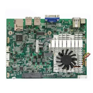
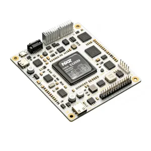
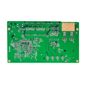
Explore our recent turnkey manufacturing runs covering critical industrial, automotive, and specialized OEM deployments.



Direct technical answers from our engineering team regarding processes, quality gates, equipment tolerances, and supply chain management.