High-performance surface mount configurations built with extreme thermal endurance, micro-BGA void rates under 8%, and automated optical and X-ray verification.
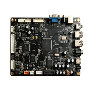

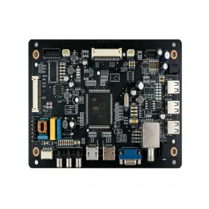
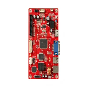

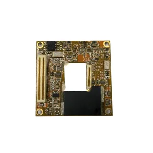
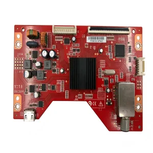
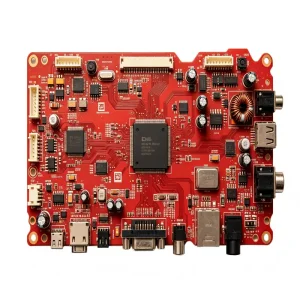
Surface Mount Technology (SMT) is no longer a simple pick-and-place commodity; it represents the central technological bottleneck and competitive differentiator for advanced electronics. With package geometries shrinking below 0.3mm pitch and multi-layer rigid-flex boards accommodating high-speed RF, automotive traction control, and portable biosensors, OEM buyers face unprecedented demands for thermal management, signal integrity, and manufacturing predictability.
The global push for handheld diagnostics, automotive sensors, and wearable IoT has driven passive component sizing from 0402 down to 0201 and 01005 / 008004 chip formats. Handling these parts requires high-precision optical alignment, nano-coated laser-cut stencils, and controlled vacuum nozzles to prevent tombstoning, skewing, and bridging defects during reflow.
High-speed computing and multi-gigahertz wireless devices utilize microvias, staggered blind/buried vias, and copper-filled VIPPO (Via-in-Pad Plated Over) architectures. Ensuring pristine solder fillet formation under heavy ground planes requires multi-zone nitrogen-purged reflow profiles that maintain strict peak temperature gradients across differential thermal masses.
Industrial power analyzers, automotive ECUs, and medical drug infusion systems cannot tolerate field failures. OEM manufacturing requires end-to-end statistical process control (SPC), 3D Solder Paste Inspection (SPI) with closed-loop feedback to the stencil printer, and 3D automated X-ray inspection (AXI) for quad-flat no-leads (QFN) and ball grid arrays (BGA).
Modern electronic manufacturing procurement professionals—whether at Fortune 500 equipment builders or high-growth tech disruptors—evaluate contract manufacturers far beyond standard cost-per-placement metrics. Supply chain integrity, engineering bandwidth, and lifecycle transparency dictate sourcing resilience.
Procurement teams require comprehensive Bill-of-Materials (BOM) health scoring. STHL actively analyzes component lifecycle states (Active, Not Recommended for New Designs, End-of-Life, Obsolete), identifying single-source IC bottlenecks and proposing drop-in, pin-compatible alternates before purchase orders are placed.
With counterfeit semiconductor incidents rising globally, enterprise buyers insist on traceability to original component manufacturers (OCM) and authorized franchised distributors (Arrow, Avnet, DigiKey, Mouser). Incoming inspection includes decapsulation analysis, XRF lead verification, and lot code cross-referencing.
Eliminating the friction between low-volume prototype verification and high-volume mass production is critical. OEM buyers demand that SMT setups run on identical feeder geometries and reflow profiles during Pilot runs as they do during 50,000-unit production orders, eliminating re-qualification costs.
Industrial and medical compliance audits necessitate serial-number-level traceability. Integrated Manufacturing Execution Systems (MES) link board barcodes to specific reel batch numbers, solder paste lot IDs, oven thermal logs, and individual operator test records for a minimum of 10 years.
A single manufacturing standard cannot address every mission profile. Automotive applications prioritize thermal cycling survivability under high vibration; medical electronics prioritize biocompliance and zero-defect longevity; and high-voltage energy storage demands creepage isolation and heavy-copper handling.
| Sector Focus | Primary Technical Challenges | SMT Manufacturing & Testing Safeguards | Certifications & Standards |
|---|---|---|---|
| Automotive Electronics (BCMs, VCUs, ADAS) | Harsh under-the-hood temperatures (-40°C to +125°C), high vibration, dynamic mechanical shear. | Automated underfill dispensing for micro-BGAs, high-Tg FR-4 / polyimide substrates, conformal coating, selective robotic soldering. | IATF 16949, AEC-Q100/Q200, IPC-A-610 Class 3 |
| Medical & Diagnostic Hardware (Infusion, Monitoring) | High component density, ultra-low leakage current, patient-safety isolation, extreme reliability. | 100% 3D AXI for hidden solder joints, automated optical inspection, ultrasonic aqueous cleaning to remove ionic residue, strict change control. | ISO 13485, FDA 21 CFR Part 820 compliant MES, IPC Class 3 |
| Industrial Automation & ESS (Robotics, Power Analyzers) | Continuous duty cycles, electrical noise immunity, high transient voltages, heavy copper planes (3oz - 6oz). | Controlled preheat zones to overcome large thermal sink dissipation, nitrogen-assisted soldering, thick-film solder stencils, potting integration. | ISO 9001, UL 796, IPC-6012 Class 2/3 |
| Smart Home & High-Volume IoT (Wearables, Voice Nodes) | Extreme miniaturization, low-power RF tuning, cost-down pressure, rapid time-to-market. | High-speed dual-beam pick-and-place lines (up to 80,000 CPH), automated RF frequency calibration, panelized test fixtures, overmolding support. | ISO 14001, RoHS 3, REACH, CE/FCC compliance |
As semiconductor lithography pushes physical boundaries, the convergence of PCBA and advanced semiconductor packaging becomes paramount. The technological trajectory of STHL Electronics aligns with industry shifts toward embedded intelligence, high-density substrate integration, and automated precision.
The integration of Package-on-Package (PoP) and multi-chip modules onto standard PCB laminates bridges the gap between silicon foundries and EMS floors. Our roadmap accommodates flux-dip micro-ball attachments down to 0.25mm ball diameter, enabling edge-AI processors to sit directly atop high-bandwidth memory.
Modern assembly lines incorporate machine learning algorithms directly into the 3D SPI and 3D AOI inspection stations. When solder paste volume deviates by more than 3% from standard distribution, automatic offsets are fed back to the stencil printer in real time, preventing solder bridging before components are mounted.
To address severe voiding limits in mission-critical power semiconductors (MOSFETs, IGBTs, GaN FETs), vacuum chamber degassing integrated within convection reflow zones reduces interfacial voiding below 5%, maximizing thermal heat sinking to ground planes.
Outsourcing electronics assembly to Asia is a strategic business decision requiring rigorous intellectual property protection, stable supply chains, and adherence to Western regulatory frameworks. STHL provides institutional guarantees that eliminate risk for overseas engineering and procurement leaders.
We execute binding Non-Disclosure Agreements (NDAs) governed by international contract law prior to file transmission. Internal network segmentation, restricted physical cleanrooms for sensitive builds, and segregated firmware burning stations guarantee that your intellectual property, schematics, and code remain completely secure.
Shipping to over 90 countries with a verified 99.5% on-time delivery record. We offer flexible Incoterms including Delivered Duty Paid (DDP), managing all export documentation, customs clearances, HTS classification, and hazardous materials declarations (UN3481/UN38.3 lithium batteries) directly to your dock.
Full documentation packages are available for European and North American market authorizations, including RoHS 3 (Directive 2015/863/EU), REACH (EC 1907/2006 SVHC screening), Conflict Minerals reporting (CMRT), and UL 94V-0 flammability certifications on all PCB core materials.
In-depth technical answers addressing design tolerances, quality gates, component lead times, and fabrication standards for sourcing directors and chief hardware architects.
Ruggedized electronic assemblies designed for harsh field environments, certified explosion-proof equipment, heavy industrial automation, and safety-critical medical solutions.
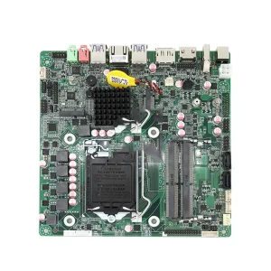

Receive a comprehensive Design for Manufacturing (DFM) assessment, component availability scoring, and precision turnkey quotation within 24 hours. Backed by certified IATF 16949, ISO 13485, and ISO 9001 systems.
