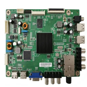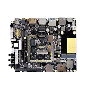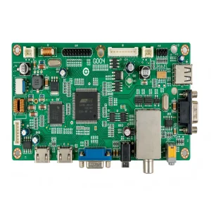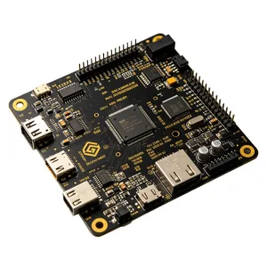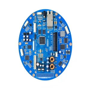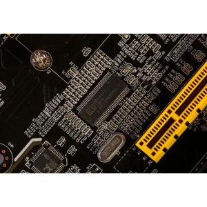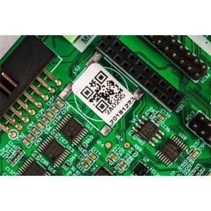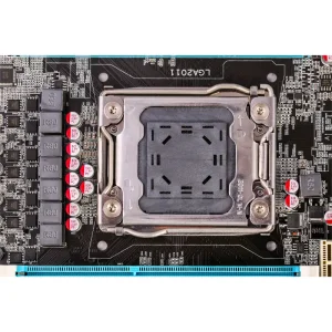
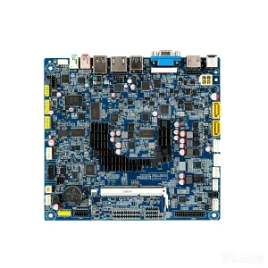
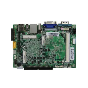
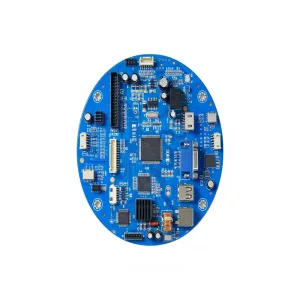
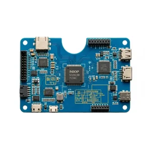
From medical imaging processing to high-frequency telecommunications, review our industrial-grade PCBA assemblies delivered for global OEM innovators.

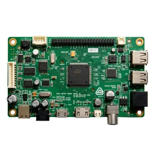
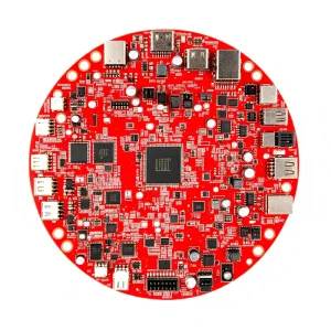
Why Tier-1 hardware OEMs, automotive innovators, and medical pioneers leverage Shenzhen’s high-velocity electronics manufacturing corridors to shorten NPI cycles and secure supply chains.
Located at the epicenter of Shenzhen’s electronic clusters, our facility sources over 500,000 qualified raw line items and micro-passive parts from over 100 franchise distributor channels like Arrow, Avnet, and Digi-Key within hours. This eliminates multi-week shipping delays typical in Western assembly environments.
Western contract manufacturers often enforce prohibitive Minimum Order Quantities (MOQs). At STHL, our multi-line layout permits seamless transitions from single-digit engineering rapid prototypes to multi-million mass runs without requalifying tooling or altering quality parameters.
Holding active IATF 16949 (Automotive), ISO 13485 (Medical), ISO 9001, and ISO 14001 credentials, STHL marries China’s production efficiency with international compliance frameworks, guaranteeing strict lot-level tracing across incoming parts, SMT lines, and outgoing carton verification.
As circuit footprints shrink and signal velocities climb into the millimeter-wave domain, surface mount processes are transitioning from mechanical assembly to materials-science engineering.
With wearables and high-density computing demanding micro-passives (01005 and 03015 metrics) and 0.3mm ball-pitch wafer-level chip-scale packages (WLCSP), our Yamaha and Fuji automated lines operate with placement accuracy tolerances within ±0.03mm under climate-stabilized chambers.
Traditional 2D optical inspection fails to catch complex solder bridging, tombstoning, or voiding under leadless QFNs and micro-BGAs. Our SMT operations deploy inline Koh Young 3D SPI (Solder Paste Inspection), 3D AOI, and high-resolution automated X-ray inspection (AXI) to maintain void rates below 10%.
Handling multi-tier Any-Layer HDI (High Density Interconnect), rigid-flex substrates, and copper coins requires sophisticated reflow thermal profile tuning beyond simple 217°C eutectic thresholds to avoid PCB warpage, delamination, and barrel cracking in microvias.
Modern mission-critical procurement demands 100% forensic trackability. Our Manufacturing Execution System (MES) links every raw reel barcode to its specific feeder slot, reflow oven temperature zone, AOI inspection image, and final laser-etched PCB data matrix serial.
Hardware reliability requirements vary widely across operating environments. Here is how our engineering protocols cater directly to specialized market demands.
Operating under severe thermal cycles (-40°C to +125°C) and harsh mechanical vibrations, our automotive SMT assemblies (e.g., ADAS domain controllers, Battery Management Systems, In-Vehicle Infotainment) follow strict IATF 16949 PPAP Level 3 documentation, conformal silicone/polyurethane potting, and automated pin-in-paste selective soldering.
From CT scanner image reconstruction units to micro-dosing drug delivery pumps and portable telemedicine terminals, STHL implements cleanroom ESD assembly cells under ISO 13485 oversight. Zero-ionic contamination is assured using inline automated deionized water washes, accompanied by 100% flying probe and functional test coverage.
5G micro-base stations, enterprise load balancers, and intelligent optical sensors demand impedance-controlled high-speed boards (up to 40 layers) utilizing Rogers, PTFE, or Panasonic Megtron laminates. Backplane thick-copper soldering ensures continuous 24/7 duty cycles without thermal fatigue.
Rigid engineering specifications verified daily on our Shenzhen production floors for procurement and hardware design auditing.
| Metric / Process Parameter | Standard Capability | Advanced / High-Density Capability |
|---|---|---|
| Min. Passive Package Size | 0201 (metric 0603) | 01005 & 03015 micro-passives |
| Fine Pitch Component Pitch | 0.40 mm pitch QFP / SOP | 0.30 mm pitch ultra-fine QFP, CSP, WLCSP |
| BGA Pitch & Ball Diameter | 0.50 mm pitch, 0.25 mm ball | 0.35 mm pitch, 0.15 mm ball (with 3D X-Ray Inspection) |
| PCB Layer Count & Stackup | 1 to 24 Layers FR-4 | Up to 48 Layers, Any-Layer HDI (1+N+1 to 4+N+4) |
| Substrate Materials | Standard FR-4, Aluminum, CEM-1 | Rogers, PTFE, Megtron 6, Polyimide Flex, Ceramic core |
| Max / Min PCB Dimensions | 50 mm × 50 mm to 510 mm × 460 mm | 10 mm × 10 mm to 1200 mm × 600 mm (LED long-boards) |
| Surface Finishes | HASL, Lead-free HASL, OSP | ENIG, ENEPIG, Immersion Silver, Immersion Tin, Hard Gold |
| Testing & Screening Methods | Visual, In-Circuit Test (ICT), 2D AOI | 3D SPI, 3D AOI, 3D AXI (X-Ray), Flying Probe, Full Functional FCT |
Navigating offshore contract manufacturing requires evaluating risk mitigation beyond unit piece costs. Overseas engineering executives qualify STHL using our transparent five-pillar governance model.
Before releasing copper to etch or cutting solder stencils, our 50+ engineers execute comprehensive Design for Manufacturability (DFM) and Design for Assembly (DFA) audits. We catch pad aspect ratio mismatches, thermal relief errors on heavy ground planes, and tombstone-prone geometries before they cause production downtime.
Intellectual property protection is legally safeguarded through non-disclosure agreements executed before any engineering collateral is exchanged. Encrypted local servers safeguard proprietary Gerber files, schematic diagrams, and secure microcontroller bootloaders during manual and automated IC programming cycles.
We provide complete turnkey procurement—including PCB fabrication, electronic component sourcing, cable harnesses, and full custom enclosure box builds. Consolidating the bill of materials cuts redundant international shipping, customs administrative costs, and vendor finger-pointing.
Clear answers to the primary technical, operational, and commercial questions asked by overseas engineering teams before initiating PCBA partnerships.
Explore more turnkey assemblies engineered and manufactured at STHL for commercial, industrial, telecommunications, and smart infrastructure deployments.