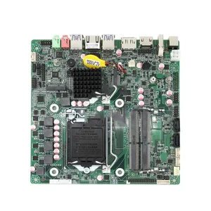
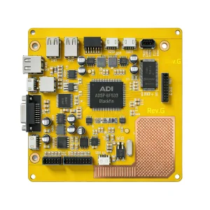
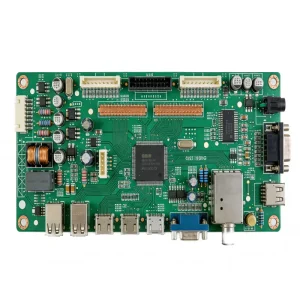
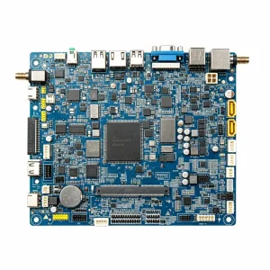
Factory-verified surface mount sub-assemblies built to IPC-A-610 Class 3 standards for automotive, power electronics, IoT infrastructure, and mission-critical devices.
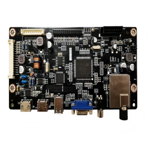
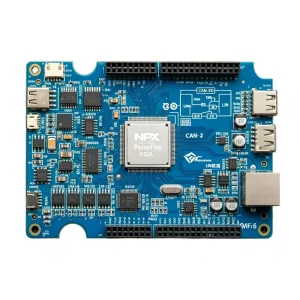
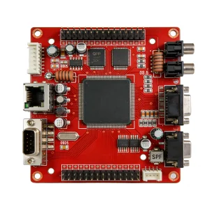

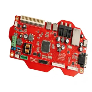
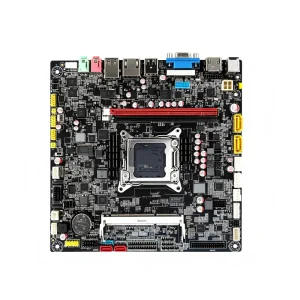
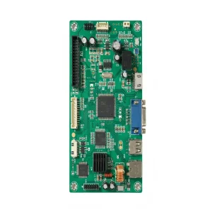
The electronics manufacturing sector has transitioned from manual board-stuffing to ultra-integrated automated surface-mount micro-assembly. Driven by ubiquitous edge AI computing, EV power systems, and high-frequency RF connectivity, modern original equipment manufacturers require PCBA contract factories capable of handling micron-level coplanarity and hyper-dense architectures.
The global demand for compact industrial edge gateways, medical body sensors, and wearable IoT has driven passive component sizing down from 0402 and 0201 packages to 01005 and metric 03015. Modern SMT factories must employ sub-micron solder paste printing, intelligent 3D SPI (Solder Paste Inspection), and zero-force chip shooters to avoid tombstoning, voiding, and micro-bridging.
Thermal gradients across heavy-copper power distributions versus fine-pitch BGA balls create massive reliability hazards. Top-tier OEM manufacturing demands 10-to-12 zone nitrogen-purged convection ovens that strictly regulate peak temperatures (liquidus at 217°C for SAC305) to ensure zero intermetallic micro-cracks and flawless joint metallurgical crystallization.
Hidden array joints like Ball Grid Arrays (BGA), Quad Flat No-leads (QFN), and Land Grid Arrays (LGA) render classic surface microscopy obsolete. Advanced PCBA contract facilities integrate inline automated 3D X-ray inspection (AXI) and high-speed multi-angle 3D AOI to calculate void percentages, pad wetting angles, and solder volume in real-time.
Precision engineered infrastructure providing agile prototyping to tier-1 mass manufacturing.
Operating in the epicentre of the world's electronics supply network (Shenzhen-Bao'an Corridor), our factory achieves an unmatched velocity of material sourcing, PCB bare-board fabrication, tooling setup, and delivery execution.
Immediate physical access to over 500,000 authentic component line items across 100+ authorized franchised distributors and component manufacturers. Short lead times for passive components, active silicon, specialized sensors, and bare FR4/Rogers substrate materials mitigate global supply bottlenecks.
Over 50 dedicated hardware and production engineers review Gerber, BOM, and Centroid databases prior to order acceptance. Every via design, component pad spacing, solder mask bridge, and stencil aperture undergoes computerized Design for Manufacturing (DFM) check to avoid production yield loss.
Agile production lines switch seamlessly from rapid 24-hour prototype proof-of-concept verification runs to high-speed mass volume manufacturing using unified SMT programming, identical feeders, and matched thermal profiles—eliminating the prototype-to-production redesign cliff.
From extreme outdoor ambient temperatures to life-saving clinical operating theaters, each OEM device ecosystem requires specialized SMT assembly techniques, conformal coatings, and potting chemistry.
Assembled in Class 100,000 clean conditions under ISO 13485 control. Implements low-leakage insulation, selective biocompatible conformal coatings, and 100% full functional testing for biological monitors, ultrasound wands, diagnostic carts, and wearable dialysis sensors.
Certified to IATF 16949 standards. Thermal cycling-resistant assemblies, AEC-Q100/200 component authentication, and automated underfill for BGA joints deployed in EV battery management systems (BMS), motor inverters, and digital infotainment head units.
Engineered for high-voltage dielectric isolation, heavy 3oz–6oz copper layers, and precision wave/selective soldering. Built to withstand continuous high ambient temperatures inside solar inverters, Power Distribution Units (PDUs), and industrial switchgear.
Impedance-controlled PCB fabrication (±5% tolerance) on low-loss Rogers, Isola, or high-Tg FR-4 laminates. Specialized shielding can placement and microstrip SMT assembly for base station repeaters, GPS telemetry receivers, and high-frequency microwave modems.
How our manufacturing lines evolve to anticipate next-generation silicon packaging, embedded components, and environmental directives.
| Technology Vector | Current Production Standard | Advanced Capability | Future Target (2026-2030) |
|---|---|---|---|
| Micro-Component Pitch | 0201 passives, 0.4mm BGA pitch | 01005 passives, 0.3mm ultra-fine BGA | 03015 passives, 0.2mm micro-bump pitch |
| Solder Paste Printing | Laser-cut electroformed stencils, 2D SPI | 3D SPI closed-loop feedback to printer | Additive jet printing, AI real-time volume adjustment |
| Inspection & Metrology | Offline X-Ray, Inline 3D AOI | Inline 3D AXI (X-Ray) + 3D AOI (100%) | Deep-learning defect classification & auto-rework |
| Substrate Technology | FR-4, Metal Core (MCPCB), Rigid-Flex | HDI Any-Layer, High-Tg Rogers/PTFE | Embedded silicon dies, ultra-thin flexible polyimide |
| Cleanliness & Solder Alloy | SAC305, Sn-Bi low-temp, RoHS compliant | Lead-Free Zero-Halogen, No-Clean IPC-Class 3 | Ultra-low voiding vacuum reflow (<5% BGA voiding) |
A dependable contract factory functions as a direct extension of your internal engineering group. We eliminate language barriers, geographical friction, and IP risk through standardized Western-aligned project governance.
Each OEM account is assigned a bilingual technical project manager and a DFM process engineer. RFQ iterations, BOM component alternatives, test fixture schematics, and production schedule adjustments are resolved without time zone lag.
Every single printed circuit board assembly is etched with a laser 2D DataMatrix barcode. Solder paste batch, reflow thermal profile history, SMT pick-and-place nozzle log, optical inspection scans, and functional test data are locked permanently into our cloud-accessible MES.
All Gerber artwork, firmware binaries, testing algorithms, and proprietary BOM structures are isolated on encrypted internal VLAN storage under strict role-based access control. Comprehensive NDAs signed prior to file intake guarantee complete commercial safety.
Direct answers to the critical engineering, quality, and logistics concerns raised by international procurement managers.
Explore additional factory assemblies manufactured under IATF 16949 and ISO 9001 quality supervision for smart energy, commercial displays, Ethernet infrastructure, and vehicle infotainment.