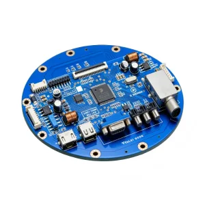
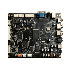
Industry Whitepaper & Precision PCBA Guide

OEM Surface Mount PCB Assembly Factories & Factory Solutions

Architecting next-generation Surface Mount Technology (SMT) ecosystems: From high-reliability micro-placement (01005 / 0.3mm BGA) to end-to-end global aerospace, automotive, and medical EMS solutions.

Industrial Applications

High-Precision Surface Mount PCB Assembly Units

Representative OEM PCBA systems manufactured for critical monitoring, mobile electronics, automotive power conversion, and clean-energy infrastructure.

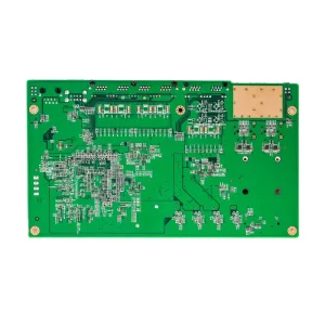
OEM Industrial Waste Gas Online Monitoring System PCB Assembly Service
Waste Gas Online Monitoring System PCBA
Explore Details
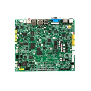
OEM Smartphone PCB Assembly STHL Manufacturer
OEM High-Density Smartphone PCBA
Explore Details
OEM Air Quality Monitor PCBA Assembly
Environmental Air Quality Monitor PCBA
Explore Details
High-Quality Gas Leak Alarm PCB Assembly
Industrial Gas Leak Alarm PCB Assembly
Explore Details
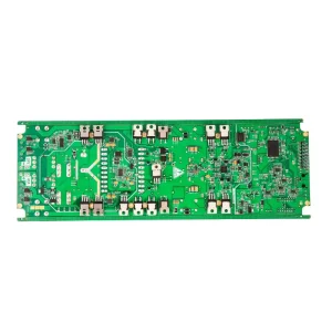
OEM On-board Charger OBC PCB Assembly Manufacturers
Automotive On-Board Charger (OBC) PCBA
Explore Details
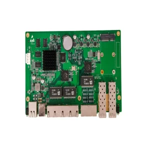
OEM DVR PCB Assembly STHL Service
High-Definition Security DVR PCBA Module
Explore Details
OEM Gas Leak Detector PCB Assembly
Commercial Gas Detection Board PCBA
Explore Details
China LED Display Board PCB Assembly
High-Brightness LED Display Control PCBA
Explore Details
Global Market Architecture

Macro Trends & Strategic Enterprise SMT Procurement

How Tier-1 original equipment manufacturers overcome geopolitical supply chain volatility, thermal bottlenecks, and microscopic package density through integrated turnkey EMS factories.

Ultra-Dense Packaging Trends

Global procurement teams face escalating demand for micro-BGA, flip-chip, and ultra-miniaturized passive passives (01005, 008004 packages). Meeting signal integrity thresholds at 50GHz+ requires OEM SMT factories equipped with sub-micron vision alignment systems and ultra-low-void vacuum reflow soldering capabilities.

Supply Chain Resiliency & Dual-Sourcing

Post-shortage electronic hardware procurement mandates proactive Bill of Materials (BOM) risk evaluations. Leading SMT assembly facilities maintain direct APIs with 100+ global distributors and silicon foundries, providing automatic life-cycle alerts, pin-compatible cross-referencing, and real-time buffer inventory.

Zero-Defect Quality Mandates

Mission-critical applications across industrial edge computing, automotive battery management (BMS), and ISO 13485 medical electronics require statistical process control (Cpk ≥ 1.67). High-tier SMT operations deploy closed-loop 3D Solder Paste Inspection (SPI) connected directly to automatic stencil printers.

10,000+
Square Meters Cleanroom Plant
7 Lines
High-Speed SMT Panasonic/Yamaha
99.5%
On-Time Global Delivery Rate
01005
Micro-Component Placement Capability
Sector Engineering

Mission-Critical Industry Engineering Solutions

Delivering precision SMT board production tuned precisely to the operating environment, regulatory clearances, and thermodynamic challenges of target sectors.

Automotive & EV Mobility

Compliant with IATF 16949 protocols. Heavy-copper FR-4 and ceramic substrates engineered for thermal cycling shock (-40°C to +150°C), conformal coatings to IPC-CC-830, and zero-void voiding profiles under high-current MOSFET packages.

Medical Diagnostics & Implants

Governed by ISO 13485 quality gates. Full traceability down to reel barcode lot numbers, Class 3 cleaning chemistries to prevent ionic contamination, and comprehensive In-Circuit and Functional Test (FCT) jigs customized per enclosure.

Industrial Automation & Robotics

Engineered for electrical noisy high-EMI environments. Surface mount assemblies featuring isolated power modules, high dielectric breakdown laminates, rigid-flex routing, and automated conformal coating to resist corrosive factory chemicals.

Telecom & High-Density Compute

High-speed HDI boards incorporating laser microvias, controlled impedance routing (±5%), and Low-loss Rogers or Megtron dielectric cores supporting multi-gigabit signal transitions without eye diagram distortion.

Engineering Specifications

Surface Mount Technology Capability Matrix

Auditable, production-verified equipment metrics representing physical assembly envelopes, precision limits, and testing capabilities.

Assembly Parameter Production Capability & Standard Advanced / High-Density Envelope
Min Component Size 0201 imperial (0603 metric) passives 01005 imperial / 008004 metric micro-passives
BGA / Ball Pitch 0.4mm pitch with standard reflow ≥ 0.25mm fine pitch with 3D X-Ray & Vacuum de-voiding
Board Types Handled FR-4 (Tg 140°C to 180°C), Aluminum Core Rigid-Flex, Polyimide, Ceramic, Rogers, PTFE, High-Copper (12oz)
Layer Count Range 1 to 24 Layers standard production Up to 64 Layers with any-layer HDI (1+N+1 to 4+N+4)
Placement Accuracy ±0.035mm (±35μm) @ 3 Sigma ±0.015mm (±15μm) for optical dies and flip chips
Max Board Dimensions 510mm × 460mm standard conveyor 1200mm × 350mm specialized long LED / backplane lines
Inspection Technology In-line 3D SPI, 3D AOI (top/bottom) High-resolution 3D AXI (X-Ray), Flying Probe, Custom FCT
Soldering Environments RoHS Lead-Free, SAC305, Clean Nitrogen (N2) Vacuum Nitrogen Reflow (<5% void area), Sn63/Pb37 for Mil/Aero
Future Roadmap

Next-Generation Technology Roadmap & AI Integration

How our surface mount PCBA manufacturing ecosystems are transitioning toward intelligent self-optimizing factories and sustainable green electronics.

AI-Driven Closed-Loop Inspection

We are deploying neural-network-backed automated optical inspection (AOI) systems that share real-time drift telemetry directly with paste printing heads. If solder volume deviates by >3%, stencil offsets calibrate automatically before bridge defects can form.

Additive Electronics & Embedded Die

Packaging innovation is moving beyond surface landing. Our engineering lines are prototyping cavity-embedded actives, direct wire bonding inside inner laminate prepregs, and hybrid 3D printed circuitry to slash total board z-height by up to 40%.

Zero-Carbon Green Electronics

Under ISO 14001 guidelines, we have incorporated bio-derived low-VOC solder flux residues, 100% recyclable halogen-free base materials, low-temperature soldering (LTS) pastes, and heat-recovery reflow ovens reducing kiln energy draw by 28%.

Global Assurance

Localized Engineering Liaison & Absolute IP Safeguards

Bridging Chinese manufacturing velocity with North American and European regulatory accountability, non-disclosure protocols, and real-time collaboration.

Comprehensive IP & NDA Protection

Design intellectual property is our clients' foundational asset. Strict non-disclosure agreements precede any technical data transfer. Firmware is flashed inside air-gapped security cleanrooms, and engineering Gerber/BOM files reside on encrypted local servers with audit trails.

24/7 Overlapping Engineering Shifts

Direct contact with English-fluent project management and DFM design engineers. We operate overlapping shift windows ensuring questions regarding bill-of-materials clarification or footprint substitutions receive actionable answers in under 4 hours.

Full Regulatory Paperwork & DDP Logistics

We supply complete Certificate of Conformance (CoC), RoHS/REACH material declarations, UL 94V-0 flammability certificates, and IPC-A-610 Class 2/3 inspection dossiers. Door-to-door Delivered Duty Paid (DDP) logistics simplify customs clearance across North America, the EU, and APAC.

Procurement Knowledge Base

Frequently Asked Questions: SMT Sourcing & Factory Audits

Exhaustive technical, contractual, and logistics answers compiled for senior electronics sourcing directors and engineering executives.

How does an OEM Surface Mount PCB Assembly factory prevent solder bridging on fine-pitch 0.3mm micro-BGAs?
Eliminating bridging on ultra-fine pitch components demands tightly coupled process stages: First, electroformed or high-precision laser-cut stencils with nano-coatings are utilized to maximize aperture paste release. Second, 3D Solder Paste Inspection (SPI) measures deposit volume and height across every pad at 100% coverage, instantly flagging any coplanarity deviation. Third, we utilize Type 4 or Type 5 solder powder pastes with optimized rheology, combined with Nitrogen-purged 10-zone reflow ovens featuring precisely calibrated soak profiles to mitigate component warpage.
What is the typical turnaround lead time for NPI (New Product Introduction) SMT prototypes vs mass production?
For rapid NPI quick-turn builds where bare boards and components are expedited, assembly can be achieved in 24 to 48 hours following DFM verification. Turnkey prototype production generally takes 7 to 10 working days, incorporating worldwide component sourcing and bare board fabrication. High-volume serial production typically follows a 3 to 4-week delivery cycle depending on raw component procurement lead times, with scheduled rolling buffer releases available for long-term contract partners.
Can your factory accommodate consign-part models, turnkey procurement, and hybrid sourcing arrangements?
Yes. We offer complete flexibility: Full Turnkey (where we manage bare board fabrication, global silicon and passive procurement, assembly, testing, and boxing); Partial Turnkey / Hybrid (where client issues high-value, proprietary programmed ICs while our purchasing team handles all standard resistors, capacitors, connectors, and peripheral ICs); and Full Consignment (where the customer delivers complete kits directly to our warehouse for automated line placement).
How are component counterfeits and reclaimed ICs eliminated in the procurement pipeline?
Our factory operates a multi-tier anti-counterfeit mitigation program compliant with AS6081 guidelines. Sourcing is strictly restricted to franchised original chipmakers (such as Arrow, Avnet, Digi-Key, Mouser) or audited Tier-1 channel partners. Incoming materials undergo internal IQC verification: microscopic package decapsulation, marking permanency acetone tests, X-ray leadframe inspection, and pin-to-pin solderability testing before warehouse intake into ESD humidity-controlled dry cabinets.
What test coverage is provided for complex high-reliability circuit boards?
We construct custom verification regimens for every assembly: 100% 3D AOI for presence, polarity, and fillet geometry; 3D X-ray inspection (AXI) for BGA/QFN void calculation; Flying Probe or Bed-of-Nails In-Circuit Testing (ICT) for passive validation; and custom Functional Circuit Testing (FCT) jigs simulating operational voltage, simulated sensor loads, RF output verification, and automated firmware flashing. Environmental stress screening (burn-in chambers and thermal shock) is also available upon request.
Turnkey PCBA Portfolio

High-Reliability Surface Mount PCBA Catalog

Integrated assemblies spanning aerospace inspection, voice recognition, clean energy inverters, building intercoms, and medical diagnostics.

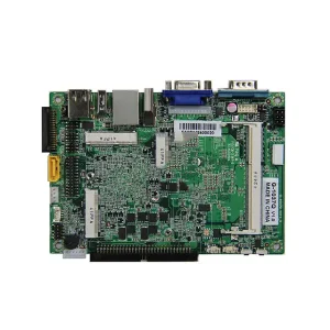
High-Quality Intercom PCB Assembly STHL
Smart Building Intercom PCBA Board
Explore Details
High-Quality Voice Assistant Device PCBA Assembly
AI Voice Assistant Audio Processing PCBA
Explore Details
China ECG Monitor PCB Assembly STHL Manufacturers
ISO 13485 Diagnostic ECG Monitor PCBA
Explore Details
China Solar Inverter PCB Assembly Manufacturer
Clean Energy Solar Inverter Power PCBA
Explore Details
High-Quality X-ray Security Inspection Machine PCB Assembly
X-Ray Security Scanner Processing PCBA
Explore Details
China In-vehicle Bluetooth Devices PCBA Assembly
Automotive In-Vehicle Bluetooth PCBA
Explore Details
OEM Energy Storage Battery Pack Management System PCB Assembly
Energy Storage Battery BMS Management PCBA
Explore Details
OEM Perimeter Protection System PCB Assembly
Perimeter Security Sensing Controller PCBA
Explore Details