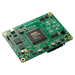
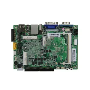
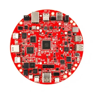
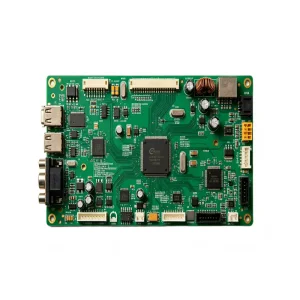
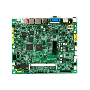
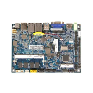
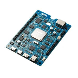
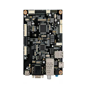
Turnkey SMT/THT PCBA configurations deployed across Japanese server farms, robotic computing platforms, and specialized embedded environments.
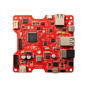
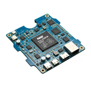
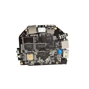
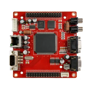
Aligning Shenzhen agile EMS throughput with Tokyo's transition toward AIoT infrastructure, automated logistics, and high-frequency cloud architectures.
The Tokyo metropolitan area represents one of the world's most concentrated clusters of advanced engineering, robotics development, enterprise data centers, and embedded hardware design. From R&D labs in Shinagawa and Akihabara to industrial automation integrators across Kanagawa and Saitama, the demand for high-reliability computer PCB assemblies (PCBA) has shifted dramatically. Legacy high-volume consumer PC manufacturing has evolved into specialized, mission-critical hardware: low-latency edge servers, industrial AI accelerators, machine vision controllers, and autonomous mobile robot (AMR) mainboards.
Japanese engineering teams maintain globally renowned standards regarding micro-defect tolerance, IPC Class 3 solder joint integrity, thermal dissipation, and extended lifespans (typically exceeding 7 to 10 years in operation). However, domestic production bottlenecks, specialized labor shortages, and skyrocketing domestic fabrication overheads compel Tokyo technology directors to establish trusted direct partnerships with certified China PCBA manufacturers capable of providing end-to-end turnkey electronic manufacturing services (EMS).
Global supply chain volatility has made component procurement a critical challenge for high-speed computer boards that require complex multi-gigabit PHYs, high-capacity DDR5 DRAM, enterprise PCIe controllers, and power management ICs (PMICs). Operating in Shenzhen—the core node of the international electronics ecosystem—STHL integrates direct Tier-1 distributor relationships (including Arrow, Avnet, Mouser, and Digi-Key) with domestic authenticated component alternatives. This allows Japanese hardware OEMs to shorten engineering verification loops while insulating their bills of materials (BOM) against sudden component lifecycle terminations.
Controlled impedance routing, differential pair matching, and micro-via HDI technology designed for up to 32-layer server and workstation motherboards.
Automated 3D SPI, inline 3D AOI, and high-resolution 3D X-ray (AXI) verification guaranteeing zero hidden solder voids beneath BGA, QFN, and fine-pitch CSP components.
Binding mutual Non-Disclosure Agreements (NDAs), encrypted Gerber handling protocols, and sandboxed firmware flashing environments for proprietary enterprise logic.
Built specifically to satisfy the exacting technical thresholds set by Japanese precision hardware procurement teams.
| Assembly Parameter | Manufacturing Capability Standard | Application in Tokyo Computing Market |
|---|---|---|
| Layer Count & Material | 1 to 32 Layers; Megtron 6, Rogers, Shengyi High-Tg FR-4, Metal Core | High-throughput Edge AI motherboards, PCIe Gen 5 daughterboards |
| Fine Pitch & Package Limits | 01005 passive chips; 0.3mm pitch BGA, PoP (Package-on-Package), WLCSP | Compact handheld industrial terminals, optical networking transceivers |
| Cleanliness & Solder Type | SAC305 lead-free, low-temperature Sn-Bi alloys; Ultrasonic & deionized washing | Full compliance with Japan RoHS, PSE, and harsh industrial environments |
| Traceability System | Full MES barcode laser engraving; component lot binding down to reel ID | Japanese enterprise audit trails, ISO 13485 medical, and IATF 16949 automotive |
| Testing Array | Flying Probe, ICT, Boundary Scan, 3D X-Ray (AXI), Custom Functional Test (FCT) | Zero-defect deployment for telecom backbones and mission-critical automation |
The deployment of high-tier computer PCB assemblies within the Kanto region is heavily differentiated across key vertical sectors:
As Japan embraces Society 5.0, the boundaries between centralized cloud computing and localized physical action are blurring. Over the next decade, Tokyo's electronic architecture demand will center on three foundational manufacturing breakthroughs:
Addressing common queries from Japanese engineering, procurement, and QA divisions regarding overseas turnkey manufacturing.
We apply IPC-A-610 Class 2 and Class 3 manufacturing workflows depending on project requirements. Our manufacturing facilities are audited under ISO 9001, IATF 16949, and ISO 13485. Every single board passes through 3D Solder Paste Inspection (SPI), automated optical inspection (AOI), and X-ray analysis for all ball grid arrays (BGA) and bottom-terminated components.
Yes. All raw materials, PCB laminates, solder wires, solder pastes, and sourced active/passive components strictly conform to the latest RoHS and REACH environmental guidelines. For finished power supply assemblies entering the Japanese market, we provide engineering support aligned with PSE (Electrical Appliance and Material Safety Law) safety criteria.
Quick-turn prototype assemblies can be produced in as little as 3 to 7 working days following engineering DFM confirmation and component readiness. Standard production batches typically require 2 to 3 weeks. Direct express air cargo from Shenzhen/Hong Kong to Tokyo (Narita or Haneda) takes only 2 to 3 business days, ensuring seamless timeline integration.
Confidentiality is fundamental to our enterprise partnerships. Prior to receiving any Gerber or BOM files, we execute standard Non-Disclosure Agreements (NDAs). Firmware programming is performed either offline on locked IC gang programmers or within isolated factory network environments with strictly logged operator access permissions.
Explore our certified electronic assemblies spanning acoustics, power conversion, environmental monitoring, and smart healthcare.