Engineered to meet rigorous industrial field deployment criteria across severe environments, heavy telemetry operations, and high-frequency edge analytics.
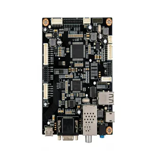
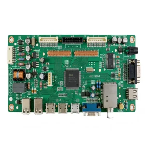

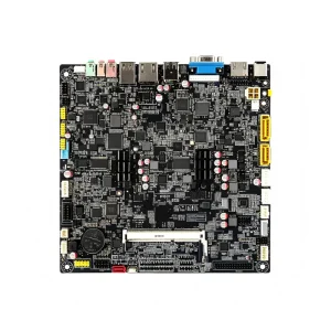
The electronic manufacturing and embedded computer market in Chile has transformed into a critical technological catalyst across Latin America (LATAM). Propelled by national digital roadmaps, automated open-pit copper mining in Antofagasta, astronomical telemetry in the Atacama, and high-yield agro-industrial corridors in the Central Valley, the demand for high-reliability computing assemblies has accelerated exponentially.
While domestic Chilean entities excel in localized system integration, hardware enclosure mechanical engineering, and localized software firmware commissioning, native Chilean surface-mount technology (SMT) fabrication infrastructure remains constrained. Local Chilean operations predominantly emphasize system maintenance, box-build integration, and rapid physical prototyping. Scalable mass production—particularly HDI (High Density Interconnect), high-speed computing motherboards, high-frequency RF transmission boards, and multilayer rigid-flex assemblies—demands strategic global integration with high-velocity electronic manufacturing hubs.
This dynamic forms a powerful supply chain synergy: Chilean technological developers lead application-specific field innovation, while advanced manufacturing hubs in Shenzhen deliver IPC Class 3 precision, comprehensive component traceability, rapid-turn bare PCB fabrication, and high-yield automated testing.
Tailored engineering and ruggedized assembly architectures optimized for Chile's unique geographical and operational conditions.
Rugged edge computing units and heavy machinery control motherboards deployed in copper and lithium extraction operations. Designed to withstand extreme mechanical vibration, high altitudes (4,000m+ above sea level), and broad thermal cycling.
Distributed power grid controllers and solar inverter control PCBA for photovoltaic installations throughout the Atacama Desert. Built with high-Tg laminate materials, conformal silicone potting, and heavy copper layers for continuous duty cycles.
Chile serves as South America's major undersea fiber-optic hub. We supply high-speed computing PCBA, server backplanes, and low-latency network routers featuring multi-gigabit differential signaling and controlled impedance tolerances.
In computing hardware manufacturing, global engineering enterprises face an unyielding triangle of challenges: miniaturization density, BOM (Bill of Materials) component volatility, and time-to-market speed. For industrial and enterprise computing equipment, a motherboard assembly can easily incorporate upwards of 3,500 individual line components, fine-pitch Ball Grid Arrays (BGAs with pitch < 0.4mm), and multilayer stackups reaching 24 to 32 layers.
Sourcing these assemblies through our state-of-the-art facility in Shenzhen gives enterprise buyers definitive advantages:
Our production facilities operate strictly under ISO 9001, ISO 13485, and IATF 16949 operational controls.
| Assembly Capabilities | Surface Mount Technology (SMT), Pin-Through-Hole (THT), Mixed Technology, Package-on-Package (PoP), Single & Double-Sided Reflow. |
|---|---|
| Component Placement Range | 01005 passives, 0201 chips, fine-pitch BGA (down to 0.35mm pitch), QFN, CSP, WLCSP, active optical connectors. |
| Supported Board Types | Rigid FR-4 (Tg 140°C to 180°C), High-Frequency (Rogers, Nelco), HDI Any-Layer, Aluminum Core, Flexible Polyimide, Rigid-Flex combinations. |
| Quality & Inspection Standards | IPC-A-610 Class 2 & Class 3, 3D SPI (Solder Paste Inspection), 3D AOI, 2D/3D Transmission X-Ray, Flying Probe, Boundary Scan, Custom Functional Testing (FCT). |
| Protective Treatments | Automated selective conformal coating (silicone, acrylic, polyurethane), potting, anti-static packaging, baked dry-packing under IPC/JEDEC J-STD-033. |
A broad array of custom-engineered assemblies serving municipal, industrial, environmental, and enterprise clients worldwide.

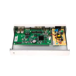
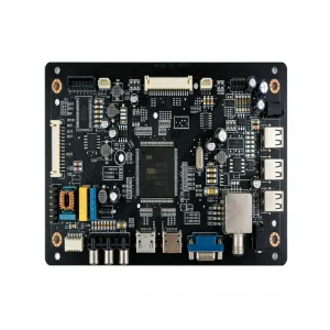
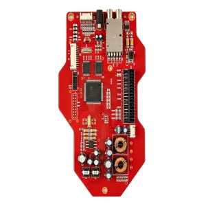
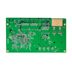
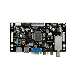
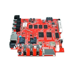
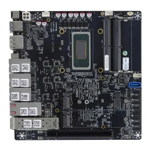
The convergence of edge AI compute, accelerated edge connectivity, and harsh-environment electronics is reshaping the global PCBA market. Over the next five years, electronic manufacturing service partners must navigate three transformative shifts:
1. Embedded Heterogeneous Computing: Modern industrial computers are rapidly migrating from generic x86 architectures to hybrid System-on-Module (SoM) topologies integrating ARM cores with specialized Neural Processing Units (NPUs). This transition requires tighter trace clearances, controlled micro-vias, and higher multi-gigahertz signal integrity protection.
2. Advanced Thermal Management: As computational throughput intensifies within sealed IP67/IP68 enclosures for mining and field telemetry in Chile, traditional copper balances are insufficient. PCBA designs increasingly integrate heavy-copper inner layers, embedded copper coins, and direct-to-chassis thermal interface materials.
3. End-to-End Component Traceability: Industrial and corporate buyers demand verifiable provenance for each mounted active and passive IC. Implementing 2D Data Matrix laser marking directly on bare circuit boards ensures complete MES ledger tracking down to individual component reel batch numbers.
Key technical, commercial, and operational insights for procurement directors and hardware engineers.
