Engineered for low latency, high thermal density, and rigorous international quality standards from prototype validation to volume ramp.
Analyzing the intersection of Central America's Silicon Hub, Free Trade Zone regimes, and high-performance contract manufacturing.
Costa Rica, specifically around San José, Heredia, and Alajuela, has evolved into a premier Latin American technology cluster. While historically recognized for semiconductor testing and medical device assembly, the regional demand for cutting-edge consumer smart devices, wearable wellness hardware, and home automation systems has surged exponentially under PROCOMER trade frameworks.
The Coyol Free Zone and America Free Zone (AFZ) provide zero-tariff corridors, fiscal incentives, and rapid logistical customs clearance. OEM and ODM brands operating in Costa Rica require agile electronics manufacturing service (EMS) partners capable of integrating directly with dual-shore frameworks, fulfilling tight inventory cycles under JIT and Kanban models.
Costa Rica generates over 99% of its electricity from renewable sources (hydro, geothermal, and wind). International consumer electronics brands deploying in the region must align with aggressive ESG metrics, requiring PCB assemblers to verify ISO 14001 compliance, RoHS/REACH material authenticity, and reduced carbon footprints throughout fabrication.
Overcoming microminiaturization, ultra-dense routing, and high-frequency RF challenges in contemporary consumer hardware.
Modern consumer smart devices demand ultra-dense HDI stack-ups (1+N+1 to any-layer interconnect). Our automated SMT lines deploy Yamaha and Panasonic high-speed mounters maintaining ±0.025mm placement accuracy, reliably shooting 01005 passive components, 0.3mm micro-BGA packages, and multi-pin CSPs under strict solder paste volume control via 3D SPI.
Consumer devices pack multi-core SoCs, 5G NR, Wi-Fi 6E/7, and Bluetooth Low Energy (BLE) transceivers within compact enclosures. We integrate ceramic, Rogers, and high-Tg FR-4 hybrid laminates, implementing controlled impedance tolerances within ±5%, buried thermal vias, and robotic selective conformal coating to ensure zero thermal throttling and signal cross-talk.
Defect escape prevention is governed through 10-zone nitrogen reflow ovens with dynamic profile logging. Every production batch undergoes multi-angle 3D Automated Optical Inspection (AOI), followed by Automated X-ray Inspection (AXI) for BGA solder voiding below 10%, In-Circuit Testing (ICT), and customer-tailored Functional Testing (FCT) before packing.
Combining China’s mature electronics supply ecosystem with rapid freight routes to Central America and global distribution nodes.
STHL partners directly with primary franchised distributors (Arrow, Avnet, Digi-Key, Mouser) alongside verified Tier-1 semiconductor foundries. Our centralized procurement engine in Shenzhen mitigates global allocation bottlenecks, provides counterfeit prevention under AS6081 protocols, and secures long-lead microcontrollers and PMICs at competitive economies of scale.
Our 10,000+ m² smart factory utilizes interconnected ERP and Manufacturing Execution Systems (MES). Every reel, solder paste lot, SMT placement machine feeder, and test log is serialized. If an anomaly arises in post-market validation, root cause analysis can trace the individual operator, reflow profile, and component batch within minutes.
Through express air lanes into Juan Santamaría International Airport (SJO) and maritime container shipping into Port Caldera or Limón, we maintain continuous delivery pipelines. We manage bonded customs handling, commercial invoicing, and DDP shipping configurations, ensuring seamless transfer directly to your San José or Free Trade Zone assembly facilities.
Rigorous frameworks designed to protect proprietary intellectual assets while ensuring worldwide commercial market compliance.
We execute legally binding Non-Disclosure Agreements (NDAs) prior to receiving Gerber, BOM, or ODB++ files. Firmware flashing is handled in isolated, encrypted production cells with cryptographic key management. Unused silicon, engineering stencils, and test logs are strictly managed to eliminate design leakage.
Our operations are certified under IATF 16949, ISO 9001, ISO 13485, and ISO 14001. Even within consumer electronics assemblies, we apply automotive-grade APQP (Advanced Product Quality Planning), FMEA (Failure Mode and Effects Analysis), and PPAP documentation to ensure consumer devices perform with mission-critical reliability.
Every PCBA manufactured for international deployment complies fully with RoHS 3 (Directive 2015/863/EU), REACH, and WEEE standards. Our engineering team assists clients with early-stage DFM (Design for Manufacturability) and preliminary EMC testing to guarantee first-pass success during official FCC, CE, and UL certification audits.
Explore our full line of turnkey manufacturing capabilities built for consumer gadgets, communications, and enterprise edge computing.
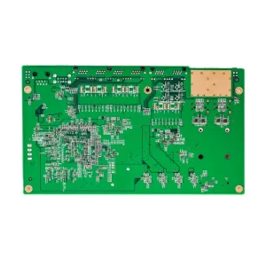
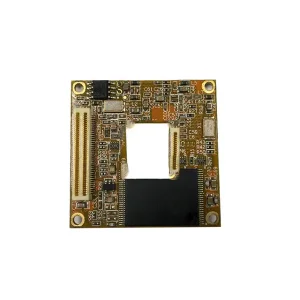
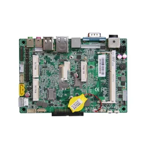
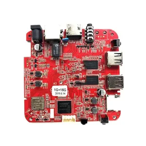
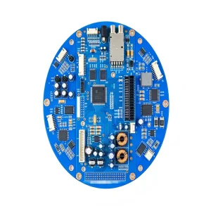
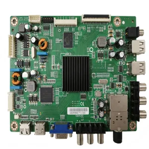
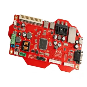
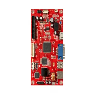
In-depth guidance for hardware engineering directors and international procurement teams sourcing PCBA for Costa Rica operations.
We supply turnkey bare PCBs, kitted SMT/THT assemblies, sub-modules, and complete box builds directly to Free Zone parks like Coyol and AFZ. By providing standardized customs export documentation, serialized packing lists, and Certificate of Conformance (CoC) reports, we enable smooth cross-border entry with zero import tariff friction under applicable trade exemptions.
Upon receiving your Gerber RS-274X/ODB++ files, bill of materials (BOM), and pick-and-place centroid data, our senior engineering staff completes a rigorous 48-hour DFM/DFA review. We analyze copper balance, trace/space clearances, solder bridge vulnerabilities, tombstoning risks, thermal relief adequacy, and component footprint accuracy before stencils are cut.
Central America presents high ambient relative humidity. We rigorously adhere to IPC/JEDEC J-STD-033 standards for handling Moisture Sensitive Devices (MSDs). Components exceeding floor-life thresholds undergo controlled nitrogen baking prior to reflow. Furthermore, we provide automated silicone, acrylic, or polyurethane conformal coatings to protect finished circuits from tropical moisture and oxidation.
We do not impose any MOQ restrictions. Our facility operates dedicated NPI (New Product Introduction) quick-turn prototype lines delivering populated boards in as fast as 24 to 72 hours following component receipt. Mass production ramps are supported across our 7 automated SMT lines with flexible batch scaling, allowing risk-free iterations before high-volume commercial runs.
Yes. In instances of End-of-Life (EOL), active allocations, or unexpected lead-time spikes on key ICs, our dedicated procurement engineers evaluate drop-in second-source alternatives or suggest minor footprint revisions to maintain delivery continuity without compromising performance or regulatory certifications.
We execute 100% 3D AOI inspection, high-resolution X-ray analysis for ball grid arrays (BGAs), In-Circuit Testing (ICT), boundary scan, and custom Functional Circuit Testing (FCT). For audio, wireless, and IoT consumer devices, we can implement automated RF calibration, Bluetooth/Wi-Fi packet verification, and firmware flash verification.
Whether you require fast-turn prototypes for proof-of-concept testing in Costa Rica or million-unit volume assembly lines, our engineering team is ready to analyze your BOM and Gerber files.
