Advanced SMT, Heavy-Copper, and Micro-Grid Telemetry Assemblies tailored for the rigorous demands of Switzerland's decentralized smart grid infrastructure and Alpine renewable deployments.
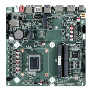
Switzerland CleanTech Energy PCBA: Smart Inversion & Grid-Tie Control Systems View Product Details
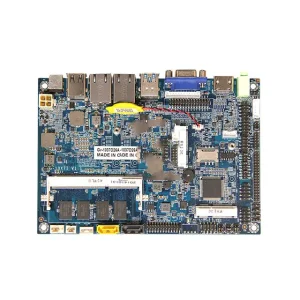
Swiss EV Fast-Charging Infrastructure: High-Current Charging Pile PCBA View Product Details

Swiss Alpine BESS Hub: Utility Energy Storage Controller PCB Assembly View Product Details

Swiss High-Altitude Photovoltaic Generation & Telemetry Monitoring PCBA View Product Details
Navigating rigorous Swiss federal energy frameworks, environmental mandates, and high-altitude micro-climates with high-tier electronic manufacturing services.
Switzerland stands at the vanguard of the European clean energy transformation. Guided by the ambitious Energy Strategy 2050 (Energiestrategie 2050) and recent federal initiatives to reinforce winter electricity security (such as the Solarexpress mandate), the Swiss confederation is rapidly replacing phased-out nuclear capacities with localized photovoltaics, micro-hydro modernization, and alpine wind installations. However, the geographic reality of Switzerland—characterized by extreme thermal differentials across cantons like Valais, Graubünden, and Bern—imposes technical demands that conventional commercial-grade printed circuit board assemblies (PCBAs) simply cannot survive.
In high-altitude alpine solar farms (e.g., Lake Muttsee floating or dam-mounted PV facilities) and decentralized Battery Energy Storage Systems (BESS) deployed across sub-zero mountain passes, power electronics encounter severe cryogenic stress (-40°C), dramatic diurnality, rapid condensation cycles, and low atmospheric pressure that increases dielectric breakdown hazards (Paschen's Law). Simultaneously, Switzerland’s dense urban hubs—from Zurich to Geneva—are deploying bidirectional EV fast-charging corridors (V2G/V2H) requiring seamless interoperability with the Swissgrid high-voltage transmission standard.
Globally, the power electronics assembly sector is pivoting from traditional silicon (Si) MOSFETs to wide-bandgap (WBG) semiconductors—primarily Silicon Carbide (SiC) and Gallium Nitride (GaN). This transition enables switching frequencies beyond 100 kHz with ultra-low thermal dissipation, drastically reducing the physical footprint of solar inverters, grid transformers, and DC fast chargers. To support Swiss Tier-1 industrial OEMs, energy equipment manufacturers, and engineering research hubs (such as ETH Zurich and EPFL spin-offs), an energy PCBA manufacturing partner must demonstrate mastery over advanced metallurgy, heavy copper trace geometries, high-temperature dielectric laminates, and automated conformal barrier chemistry.
Zero-defect electronic assemblies conforming strictly to EN 50549-1/2 grid connection codes, IEC 62109 safety benchmarks, and RoHS/REACH non-hazardous substance protocols mandatory across the EU/EFTA zone.
Proprietary polymer potting and dual-pass fluoropolymer/silicone conformal coatings safeguarding critical traces against hygroscopic condensation, thermal cycling (-40°C to +105°C), and micro-cracking.
Deterministic bus communication PCBAs incorporating isolated CANopen, Modbus TCP, EtherCAT, and IEC 61850 protocols for real-time edge telemetry and responsive sub-station load management.
Addressing the critical physical limitations of current density, thermal transfer, and high-frequency parasitic inductance in high-voltage energy assemblies.
Modern renewable energy systems generate unprecedented heat flux across ultra-compact form factors. In heavy-duty Swiss battery energy storage and bidirectional charging piles, power density often exceeds 50 W/cm² around central switching bridges. Conventional FR-4 substrates (thermal conductivity ~0.3 W/m·K) are insufficient to prevent thermal throttling or catastrophic junction failure. Our technical roadmap incorporates Direct Bonded Copper (DBC), Insulated Metal Substrates (IMS) with aluminum/copper base plates, and hybrid multi-layer stackups integrating ceramic-filled dielectric prepregs boasting thermal conductivities up to 3.0 to 8.0 W/m·K.
Furthermore, the steep dv/dt switching transients inherent in SiC and GaN devices (often exceeding 50 V/ns) induce severe electromagnetic interference (EMI) and excessive ringing across stray trace inductances. Our front-end engineering teams run comprehensive Design for Manufacturing (DFM) and Design for Electromagnetic Compatibility (DF-EMC) simulations prior to SMT fabrication. We optimize kelvin source connections, minimize high-frequency switching loop paths through balanced coplanar waveguide routing, and integrate embedded capacitive planes to damp parasitic resonance.
| Engineering Parameter | Standard Renewable Assembly | Advanced Alpine/Mission-Critical Specification |
|---|---|---|
| Base Copper Thickness | 1 oz to 3 oz (35 µm - 105 µm) | 4 oz up to 12 oz (140 µm - 420 µm) for heavy busbars |
| Substrate Core Formats | High-Tg FR-4 (Tg > 170°C, Td > 340°C) | Aluminum-IMS, Copper Core, Ceramic (Al2O3/AlN), Rogers 4350B Hybrids |
| Solder Alloy & Void Control | SAC305 (Sn96.5Ag3.0Cu0.5), IPC Class 2 (<25% void) | High-Reliability Innolot / Sn-Sb alloys, Vacuum Vapor Phase (<5% QFN/BGA voiding) |
| Dielectric Breakdown Voltage | 1,500 V DC Isolation | 5,000 V AC / 10,000 V DC Isolation with Creepage Slotting & CTI > 600V (FR-4 Class 0) |
| Surface Protection Finishes | Lead-Free HASL / Standard ENIG | Electroless Nickel Immersion Gold (ENIG 3-5 µin Au), ENEPIG, Immersion Tin/Silver |
| Environmental Barrier Application | Single-dip Acrylic Conformal Coating | Automated Selective Robotic Spray (Silicone / Polyurethane / Parylene) to IPC-CC-830 |
Engineered to conquer the unique physical, electrical, and geographical realities of the Swiss Confederation.
Deployed in extreme elevations (2,000m+) such as the Glarus Alps and Valais peaks. Optimized for bifacial albedo gain, high UV radiation degradation immunity, and thermal shock during rapid weather swings.
Engineered for high-throughput DC chargers along the A1 and A2 Gotthard transit corridors. High MTBF control units capable of sustaining constant 350 kW liquid-cooled charging cycles without galvanic degradation.
Equipping Swiss cantonal energy utilities with microgrid tie-in PCBA controllers. Facilitates autonomous islanding, instantaneous frequency balancing, and telemetry linkage to Swissgrid load centers.
Explore our specialized PCB assembly configurations manufactured under IATF 16949, ISO 9001, and ISO 14001 certified production pipelines for Swiss and international applications.

Swiss Alpine Wind Turbine Main Controller & Pitch Actuator PCBA View Product Details

Swiss Hybrid Grid-Tied Solar Inverter & MPPT PCB Assembly View Product Details

Swiss Intelligent BMS: Multi-Cell Active Balance PCB Assembly View Product Details

Swiss High-Voltage BESS Pack Management & Protection PCBA View Product Details
Swiss Municipal Off-Grid Solar Lighting & IoT Controller PCBA View Product Details
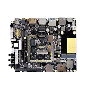
Swiss Urban Micro-Mobility: High-Torque BLDC Motor Controller PCBA View Product Details
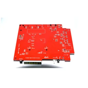
Swiss Precision Industrial Power Tool Management Module PCBA View Product Details
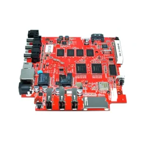
Swiss Distributed Multi-Source Generation Control System PCBA View Product Details
Automated optical, radiographic, and environmental stress screening designed to eliminate field failure risks across 25-year operational lifespans.
For Swiss industrial clients, an unpredicted field failure in an alpine inverter or isolated substation translates to exorbitant maintenance costs, helicopter transport fees, and grid disconnection penalties. At our Shenzhen manufacturing complex, quality governance is anchored in strict adherence to IPC-A-610 Class 3 standards (the highest threshold for high-performance and harsh-environment electronics) and the automotive zero-defect discipline governed by IATF 16949.
Every energy board moving through our high-speed SMT lines is subjected to inline 3D Solder Paste Inspection (SPI), multi-angle 3D Automated Optical Inspection (AOI), and high-resolution 3D Automated X-ray Inspection (AXI). Our AXI methodology scrutinizes the internal solder joints of Quad Flat No-leads (QFNs), Ball Grid Arrays (BGAs), and power MOSFET bottom pads, ensuring thermal and electrical void ratios remain securely below 5%—well above typical commercial tolerance levels.
In addition, all finished PCBAs undergo rigorous post-assembly screening: dynamic ICT (In-Circuit Testing), custom multi-channel Functional Testing (FCT), 100% high-potential (Hi-Pot) insulation stress verification, and environmental burn-in cycling within thermal chambers (-40°C to +85°C with 95% relative humidity) to precipitate early-life latent component failures before oceanic or air shipment to Switzerland.
Laser-etched 2D data matrix codes on every circuit board link down to individual silicon reel batch IDs, paste inspection volumetrics, reflow temperature profiles, and operator station logs for 15+ years.
Ultra-fine placement accuracy (±15 µm @ 3-sigma) for compact GaN/SiC power stages, ensuring balanced thermal pad coverage, minimum solder balling, and void-free thermal conduction interfaces.
Direct door-to-door DDP logistics serving Zurich, Geneva, Basel, and Bern, fully backed by comprehensive COC (Certificate of Conformance), material safety datasheets, and UL94-V0 flammability certificates.
Critical technical insights covering compliance, heavy copper management, logistics, and prototyping for the Swiss energy sector.
We deploy high-Tg (180°C+) low-CTE dielectric laminates matched with specialized solder alloys (such as Innolot) engineered to resist thermal fatigue. Assemblies receive precision robotic conformal coating or selective polyurethane potting to seal against condensation, meeting Swiss alpine environmental stress expectations.
We routinely fabricate and assemble inner and outer layers with 4 oz to 10 oz copper (with capabilities scaling up to 12 oz on specialized runs). Our automated selective wave soldering and high-thermal-mass reflow ovens ensure complete through-hole barrel fill and flawless wetting on heavy busbar solder pads.
Yes. Our in-house engineering team designs custom FCT (Functional Circuit Test) fixtures that simulate dynamic grid loads, overvoltage spikes, islanding detection response, and real-time CAN/Ethernet telemetry, ensuring your boards satisfy EN 50549 standards prior to shipment.
Turnkey quick-turn prototypes can be assembled and fully inspected in as few as 5 to 7 business days following DFM file freeze and component kit verification. We offer express air freight via DHL/FedEx directly into Zurich (ZRH) or Geneva (GVA) with typical customs transit of 3 to 4 days.
