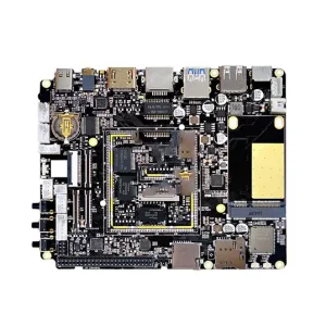
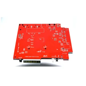
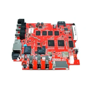
Turnkey electronic manufacturing powering the UK capital’s microgrids, public EV networks, and renewable power infrastructure.
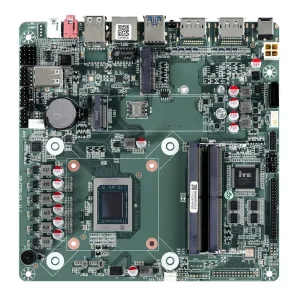
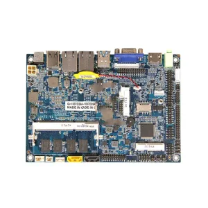


Empowering system integrators across the M25 corridor and Tech City with industrial-grade electronic assembly tailored for decarbonization and resilience.
Greater London Authority's ambitious net-zero target places unprecedented technical demands on urban distributed networks. We engineer high-frequency power electronics and localized sub-station telemetry PCBA that deliver ultra-low harmonic distortion and exceptional thermal stability under dense city conditions.
The capital's Ultra Low Emission Zone expansion accelerates EV hub deployment across Canary Wharf, Stratford, and Heathrow logistics arteries. Our high-voltage DC fast-charger control boards incorporate reinforced creepage distances, conformal potting, and IEC 61851-compliant protocol control.
London's legacy commercial properties demand modular Battery Energy Storage Systems (BESS) for grid-balancing and peak shaving. We assemble multi-layer BMS circuit boards featuring sub-millivolt sampling precision and real-time active cell balancing to maximize multi-megawatt battery life cycles.
Leveraging intelligent surface-mount technology (SMT) and automated optical/X-ray inspection to deliver mission-critical reliability for British engineering enterprises.
Ensuring complete product conformity from bare board fabrication to final box-build integration.
Deploying high-density switching circuits within London’s RF-congested urban landscape requires precision EMI shielding and trace routing. Our engineering team conducts stringent pre-compliance reviews against BS EN 61000-6-3 (Residential/Light Industrial) and BS EN 61000-6-2 (Industrial Immunity) to prevent costly redesigns.
Every assembly line operates under rigorous lead-free protocols, fully compliant with UK RoHS regulations. For mission-critical energy installations, we support IPC Class 3 manufacturing, requiring complete barrel fill on through-holes, tight component tolerances, and total process auditability.
London's humid outdoor operating environments necessitate superior moisture and condensation defense. We offer automated robotic conformal coating (acrylic, silicone, polyurethane) and high-conductivity thermal resin potting, protecting sensitive sensing tracks against outdoor oxidation, road salting, and temperature swings.
Each PCBA receives a high-resolution 2D data-matrix barcode. From lot-level semiconductor verification to reflow oven thermal curves, London clients receive comprehensive quality documentation and certificates of conformity (CoC) for uncompromised safety audits.
Architecting higher efficiency, compact form factors, and edge-intelligence for London’s future infrastructure.
Expert answers addressing customs logistics, rapid prototyping, and production verification for the UK market.
We provide full DDP (Delivered Duty Paid) shipping directly to your London headquarters or logistics hubs across Kent, Essex, or Berkshire via express air freight (DHL/FedEx/UPS) within 3-5 business days, handling all customs clearance and VAT documentation seamlessly.
Yes. Our in-house engineering team of 50+ specialists reviews your Gerber, BOM, and pick-and-place files prior to quoting. We identify obsolete or high-lead-time components and suggest pin-to-pin, commercially available alternatives through our 100+ franchised distributors.
Beyond automated 3D AOI and X-ray inspection, we offer In-Circuit Testing (ICT), Flying Probe tests, customized Functional Testing (FCT), Dielectric Withstand (Hi-Pot) testing up to 5kV, and thermal burn-in aging under loaded conditions to guarantee zero field failures.
We maintain an agile "No MOQ" policy. You can build 5-10 prototype boards for fast bench testing in London and seamlessly scale to 100,000+ units on identical high-speed Yamaha and Fuji SMT lines with complete process parameter migration.
Explore our complete manufacturing ecosystem spanning utility wind controls, solar inverters, battery management, and smart mobility electronics.