Engineered to meet rigorous Japanese Industrial Standards (JIS) and extreme factory floor conditions.
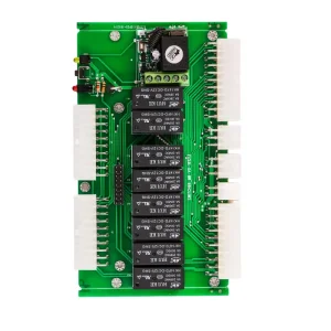
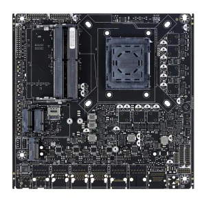

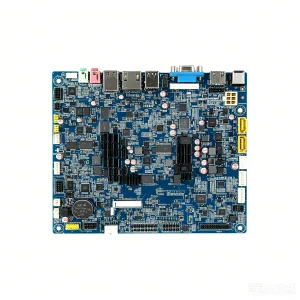
A deep dive into Kansai's precision engineering demands, from Higashiosaka SME clusters to Sakai mega-automation plants.
The Greater Osaka industrial belt, anchoring the Keihanshin metropolitan region, has historically served as the technological crucible of Japanese machinery, robotics, and advanced factory automation. Driven by the philosophy of Monozukuri (the art and science of craftsmanship), Osaka-based OEMs have engineered benchmark systems across multi-axis Computer Numerical Control (CNC) machinery, programmable logic controllers (PLCs), high-torque servo drives, and heavy power transmission infrastructure.
In locations spanning from the dense high-precision machining hubs of Higashiosaka to the coastal chemical and advanced materials clusters in Sakai and Osaka Bay, the demand for industrial control electronics has shifted drastically. Modern industrial installations no longer tolerate standard commercial circuit boards. High electromagnetic interference (EMI) generated by heavy inductive motor loads, constant structural micro-vibrations, high ambient humidity during Osaka's monsoon months, and corrosive airborne particulates necessitate PCB assemblies engineered to military-adjacent tolerances.
Furthermore, the rapid transition toward Smart Factories (Society 5.0 in Japan) demands that legacy programmable controllers be retrofitted or replaced with Edge AI-enabled microcomputers capable of executing real-time kinematic calculations, vibration harmonic sensing, and predictive maintenance algorithms right on the manufacturing line.
As tier-one and tier-two industrial component manufacturers across Osaka look to decouple from vulnerable single-source logistics, they require agile, highly certified contract manufacturing partners. STHL bridges the exacting standards of Japanese engineering oversight with the speed, technical breadth, and scalable component supply lines of premier electronics manufacturing services.
Architectural considerations for ensuring 24/7/365 uninterrupted uptime in demanding industrial operating envelopes.
Industrial servo amplifiers and motor drives dissipate massive heat flux. We employ 3oz to 6oz heavy copper inner and outer layers, copper-filled thermal via arrays under power MOSFETs, insulated metal substrates (IMS), and direct aluminum heat sink attachment protocols to avoid junction breakdown.
Factory environments in Osaka face intense electrical transients from variable frequency drives (VFDs) and arc welding equipment. Our engineering layout applies strict guard traces, isolated grounding planes, ferrite bead placement, and compliance with IEC 61000-4-4 (EFT/Burst) and IEC 61000-4-5 (Surge).
Osaka Bay installations risk salt-fog corrosion and condensation. We provide robotic selective conformal coating utilizing UL 94V-0 rated acrylics, polyurethanes, and silicones (IPC-CC-830C compliant), followed by automated UV blacklight inspection to ensure complete capillary coverage around dense SMT pins.
Unlike consumer electronics with 12-month upgrade cadences, Osaka industrial control machinery must maintain operational maintenance lifespans of 10 to 20 years. A core failure point in industrial operations is the sudden end-of-life (EOL) of critical microcontrollers, gate drivers, or analog-to-digital converters (ADCs). Our supply chain engineering team integrates directly with 100+ global tier-one distributors, monitoring Product Change Notifications (PCNs) and End-of-Life notices. We proactively conduct pin-compatible drop-in alternative qualification, verify silicon revision notes, and perform re-engineering reviews long before physical assembly lines are halted.
Comprehensive manufacturing parameters calibrated to satisfy Japanese industrial OEM standards.
| Manufacturing Parameter | STHL Engineering Benchmark | Industrial Application Context |
|---|---|---|
| Layer Count & Substrate Materials | 1 to 32 Layers; High-Tg FR4 (Tg > 170°C), Halogen-free, Rogers, Ceramic, Aluminum Base | Prevents delamination during sustained 85°C enclosure temperatures in continuous duty industrial robotics. |
| Copper Foil Thickness | 0.5 oz up to 6 oz (Outer & Inner layers) | Handles high peak in-rush currents in motor drives, inverters, and heavy relays without trace burnout. |
| Minimum SMT Pitch & Passives | 01005 passives, 0.3mm pitch BGA / CSP, 0.4mm pitch QFP | Enables high-density placement for miniaturized edge-computing PLCs and compact CNC remote I/O heads. |
| Surface Finishing Options | Electroless Nickel Immersion Gold (ENIG), ENEPIG, Immersion Tin, Hard Gold for Edge Connectors | Guarantees zero gold embrittlement and maximizes solder joint shear strength under continuous vibration. |
| Inspection & Verification Protocol | 3D Solder Paste Inspection (SPI), Inline 3D AOI, 3D Automated X-Ray (AXI), Flying Probe, In-Circuit Test (ICT) | Eliminates solder bridging, tombstones, and voids underneath non-visible BGA/QFN thermal pads (< 15% voiding). |
| Environmental & Functional Testing | Custom Bed-of-Nails FCT, Boundary Scan, Thermal Shock (-40°C to +125°C), High-Pot Isolation (up to 5kV) | Validates dielectric breakdown thresholds and proves functional execution prior to crating and export. |
Specific hardware deployment use-cases where high-integrity assembly prevents costly industrial downtime.
Osaka’s manufacturing landscape is heavily reliant on automated robotic welding, pick-and-place, and painting units. These robotic systems require high-density, multi-axis motor driver PCBA modules capable of handling dynamic torque spikes while maintaining microsecond-level optical encoder feedback loops. Our assemblies incorporate flex and rigid-flex technology, allowing controller boards to endure millions of bending cycles inside robot joints without copper micro-cracking.
The Port of Osaka and nearby Kansai International Airport logistics freight terminals operate massive autonomous guided vehicle (AGV) fleets and automated container handling cranes. On-board vehicle control units (VCUs), radar sensor fusion boards, and power distribution modules must operate in salt-laden ocean air with zero tolerance for moisture-induced circuit leakage. Our sealed conformal coating and automated potting processes safeguard these systems against marine degradation.
Kansai's industrial transition toward decarbonization involves widespread installation of multi-megawatt battery energy storage systems (BESS). We assemble master-slave Battery Management System (BMS) controllers, high-voltage isolation measurement boards, and grid-tie inverter PCBA assemblies capable of handling sustained 1500V DC working potentials with strict creepage and clearance distances compliant with IEC 60664-1.
Osaka’s die-and-mold machining manufacturers demand nanoscale interpolation accuracy. Controller PCBA backplanes demand extreme clock synchronization, controlled impedance routing (single-ended 50Ω, differential 90Ω/100Ω ±5%), and microvia-in-pad plating to eliminate parasitic capacitance and inductance that could distort high-speed optical encoder signaling.
Conforming to the rigorous standards of Japanese corporate procurement.
Exporting industrial machinery or deploying systems within Japan requires stringent adherence to national electrical regulations. We manufacture in compliance with Japanese Industrial Standards (JIS C 5012 for test methods of printed wiring boards, and JIS C 61000 series for electromagnetic compatibility). Furthermore, for industrial power electronics crossing into the jurisdiction of the Ministry of Economy, Trade and Industry (METI), we ensure component-level PSE certification where applicable, alongside comprehensive RoHS 3, REACH, and Conflict Minerals reporting.
Our engineering support team interfaces with bilingual technical documentation, ensuring that bills of materials (BOM), CAD centroids, and engineering change notices (ECN) align precisely with Japanese client conventions, preventing misinterpretations during design-for-manufacturability (DFM) verification.
In mission-critical industrial manufacturing, accountability cannot end at shipment. Our Bao'an Shenzhen production center operates a state-of-the-art Manufacturing Execution System (MES) tightly coupled with automated SMT placement stations. Every PCB is laser-marked with a high-density 2D DataMatrix barcode at the bare-board stage.
Throughout the manufacturing pipeline, our system records:
Adapting next-generation wide-bandgap semiconductors, embedded edge intelligence, and low-carbon assembly.
Wide Bandgap (WBG) semiconductors offer ultra-fast switching frequencies and superior thermal conductivity. We have perfected SMT mounting profiles and minimized loop inductances for discrete Gallium Nitride (GaN) and Silicon Carbide (SiC) power stages, eliminating parasitic oscillations in next-gen industrial inverter drives.
Modern industrial control boards increasingly host Neural Processing Units (NPUs) running localized Computer Vision and acoustic inference. Our SMT capabilities support multi-layer ultra-dense HDI stack-ups (1+N+1 to 3+N+3 with staggered and stacked laser microvias) for compact BGA-packaged neural accelerators.
To reduce thermal stress on fragile high-performance sensors and lower the cumulative carbon footprint of industrial assembly, we have integrated advanced Bismuth-based low-temperature solder paste alloys, decreasing peak reflow chamber thermal shock by more than 30°C while maintaining vibration shear reliability.
Direct answers for purchasing managers, quality assurance auditors, and hardware engineering leaders.
Engineered for high reliability, long service lifespans, and mission-critical uptime across industrial sectors.



Send your Gerber files, BOM, and assembly schematics today. Our engineering specialists will return comprehensive DFM feedback and a transparent turnkey quotation within 24 hours.
Send Inquiry Now