Explore active production builds engineered with zero MOQ, ultra-dense component integration, and automated 24-48 hour prototyping cycles.
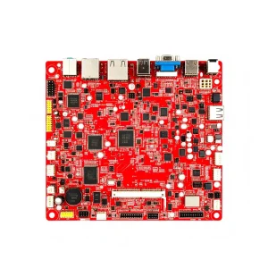
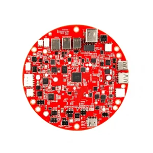
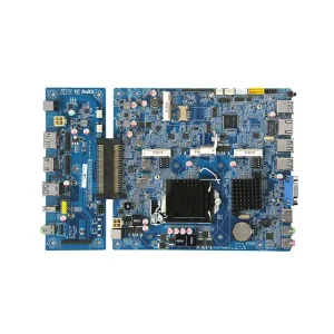

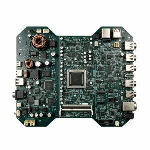
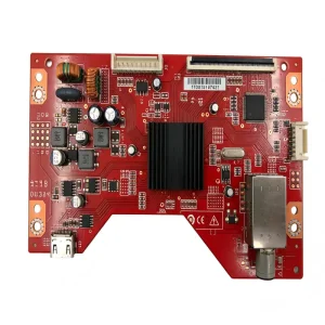
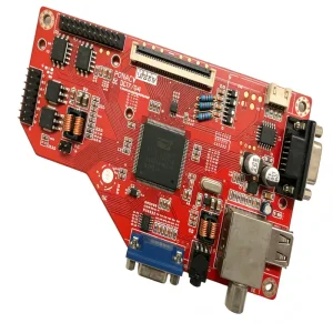
In an era defined by aggressive time-to-market windows, compressed hardware revision cycles, and escalating technological complexity, fast-turnaround PCB fabrication and EMS assembly have ceased to be purely logistical metrics; they are strategic competitive levers.
Global original equipment manufacturers (OEMs) and fabless hardware pioneers are moving from quarterly prototype validation to agile, bi-weekly engineering sprints. China's fast turnaround ecosystem bridges design iterations with rapid 24-hour quick-turn bare boards and 48-hour fully assembled SMT prototypes, eliminating idle engineering wait time.
High-Density Interconnect (HDI) structures with microvias, staggered/stacked laser vias, and ultra-fine trace/space (down to 2.5/2.5 mil or sub-50μm via mSAP) are shifting into quick-turn pipelines. Prototypes can no longer compromise on layer count or dielectric thickness merely to expedite turnaround time.
Modern quick-turn fabrication relies on real-time automated Design for Manufacturability (DFM) and Design for Assembly (DFA) cloud rule engines. By scrubbing Gerbers, IPC-2581, and ODB++ packages within minutes, potential copper slivers, annular ring breakouts, and solder-mask bridging hazards are pre-empted before copper lamination begins.
Procurement executives and supply chain directors across North America, the European Union, Japan, and Australia face multifaceted challenges when sourcing fast-turnaround printed circuit assemblies.
Dispersed supply chains that split PCB bare-board fabrication, BOM sourcing, and SMT assembly across three separate vendors introduce handoff latencies, tariff friction, and finger-pointing during yield failures. Enterprise buyers mandate an integrated EMS partner with one schedule, one contract, and unified quality assurance.
In high-mix, quick-turn production, counterfeit electronic components pose catastrophic risks. Procurement demands traceable vendor pipelines through authorized distributors (Arrow, Avnet, DigiKey, Mouser) backed by incoming inspection: decapsulation, XRF elemental screening, and heated chemical testing.
Mission-critical procurement necessitates lot-level serialization. Our Manufacturing Execution System (MES) maps every SMT reel, solder paste reflow thermal profile, optical inspection (AOI) record, and X-ray radiograph directly to the unit's serialized 2D data-matrix barcode.
Fast turnaround cannot exist in a vacuum that cannot scale. Prototypes produced on quick-turn lines must utilize standard panellization geometries, pick-and-place feeders, and reflow recipes that translate without re-engineering into tens of thousands of mass-production units.
Customized quick-turn methodologies engineered to meet stringent thermal, dielectric, and mechanical constraints across complex industrial ecosystems.
IATF 16949 compliant high-copper heavy-current boards (up to 12oz copper) for Battery Management Systems (BMS), On-Board Chargers (OBC), and motor inverter controls. Designed for extreme vibration resilience, thermal cycle endurance (-40°C to +150°C), and IPC Class 3 solder fill requirements.
ISO 13485 certified prototyping for cardiac monitors, ultrasound beamformers, and digital X-ray processing boards. Incorporates ultra-thin flex/rigid-flex substrates, non-magnetic surface finishes (ENEPIG), Class 3 cleanliness controls, and automated ionic contamination testing.
Turnaround solutions leveraging low-loss RF laminates (Rogers 4350B, Taconic, Megtron 6/7) combined with FR-4 hybrid stackups. Backdrilled via stubs to eradicate signal reflections in 112 Gbps PAM4 channels, tightly controlled 50Ω single-ended and 100Ω differential impedance ±5%.
Fabrication under IPC-6012DS Class 3/A with wrapped copper plating at knee-to-barrel interfaces. Polyimide materials for elevated Tg (>250°C), conformal coating (polyurethane, silicone, parylene) to prevent tin whiskers and moisture ingress in high-altitude environments.
Ultra-high layer count bare boards (up to 32 layers) accommodating micro-pitch BGAs (0.35mm pitch). Advanced planarized VIPPO (Via-in-Pad Plated Over) processes enabling uncompromised routing density directly underneath ultra-large AI neural processing units.
Aluminum, copper-core IMS (Insulated Metal Substrates) and embedded ceramic heat slug boards tailored for gallium nitride (GaN) and silicon carbide (SiC) power switching modules with exceptional thermal conductivity (>8.0 W/m-K).
Engineered to exceed IPC Class 2 and Class 3 manufacturing tolerances across bare-board fabrication and automated surface mount placement.
| Manufacturing Parameter | Standard Quick-Turn Capability | Advanced / Frontier Limits | Quality Verification Standard |
|---|---|---|---|
| Layer Count Capability | 1 to 16 Layers (24-72h) | Up to 32 Layers (<5 days) | IPC-6012 Class 3, Cross-section X-ray |
| Minimum Trace / Space (L/S) | 3.0 / 3.0 mil (75μm / 75μm) | 2.5 / 2.5 mil (mSAP process) | AOI (Automated Optical Inspection) |
| Microvia / Mechanical Hole | Mechanical: 0.15mm (6 mil) / Laser: 0.10mm | Laser Microvia: 0.075mm (3 mil) | Micro-CT & Impedance TDR Profiling |
| Surface Finishes | Lead-Free HASL, ENIG, OSP | ENEPIG, Immersion Tin/Silver, Hard Gold | XRF Plating Thickness Verification |
| SMT Component Range | 0201 passives, 0.4mm pitch QFP/BGA | 01005 passives, 0.3mm pitch micro-BGA | 3D Solder Paste Inspection (SPI) & 3D AOI |
| BGA Solder Joint Verification | Automated 2D Transmission X-Ray | 3D AXI (Automated X-Ray Inspection) with CT | Voiding < 10% per IPC-7095 Class 3 |
| Turnaround Speed (Bare Board) | 2L: 24h • 4-6L: 48h • 8-12L: 72h | Emergency Same-Day 12h Cycle (2L) | 100% Netlist Flying Probe / Bed of Nails |
Combining international engineering standards with rapid customs facilitation and end-to-end regulatory adherence.
STHL maintains continuous active certifications for IATF 16949 (Automotive), ISO 13485 (Medical Devices), ISO 9001 (Quality Management), and ISO 14001 (Environmental Safety). Every build conforms to UL 94V-0 flammability ratings and RoHS / REACH directives.
Engineering teams stationed in Shenzhen collaborate with client procurement and hardware teams across Silicon Valley, Munich, London, Tokyo, and Sydney. Real-time DFM resolution via automated collaborative engineering portals reduces file-approval latency to under 60 minutes.
All schematic, Gerber, and proprietary firmware payloads operate within air-gapped, encrypted networks guarded by strict Non-Disclosure Agreements (NDAs). Hardware security modules (HSMs) and automated MAC/Key flashing stations guarantee firmware integrity without exposure.
Leveraging direct air corridors from Shenzhen and Hong Kong logistics hubs via DHL, FedEx, and UPS Priority. Prototypes cleared through customs reach European and North American engineering benches within 24 to 48 hours from factory release.
Anticipating next-generation electrical packaging architectures, embedded active components, and automated predictive manufacturing.
Transitioning from traditional chemical subtractive etching toward Modified Semi-Additive Processing (mSAP). This unlocks trace geometries down to 20μm/20μm for next-generation mobile devices, wearables, and multi-chip module (MCM) substrate-like PCBs (SLP) within standard quick-turn frameworks.
Embedding discrete capacitors, resistors, and bare silicon dies directly within internal PCB core prepregs. Eliminates parasitic inductance, radically improves high-frequency power distribution network (PDN) impedances, and frees outer layers for ultra-dense sensor layouts.
Real-time machine vision and neural-network reflow ovens that adjust 10-zone thermal conveyor velocities dynamically based on thermal mass calculations from board Gerber copper density maps, eliminating tombstoning and BGA head-in-pillow defects in rapid prototyping.
Clear, definitive engineering answers addressing the operational, manufacturing, and logistical nuances of fast-turnaround PCB and PCBA production.
Engineered to rigorous environmental and mechanical standards, backed by full MES process traceability and global delivery.
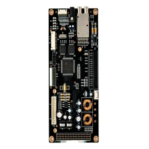
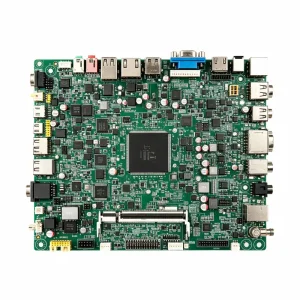

Send your Gerber files, BOM, and assembly drawings today. Our senior engineering team will return a comprehensive DFM audit, impedance analysis, and guaranteed quick-turn quotation within hours.
