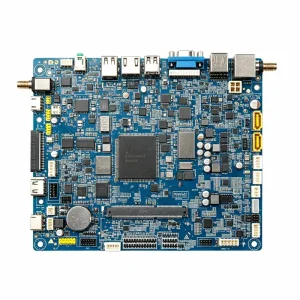
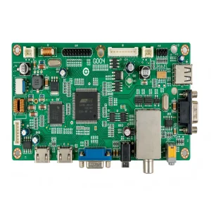
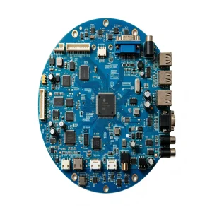
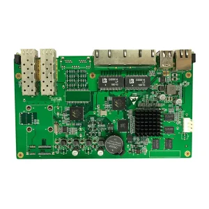
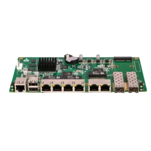
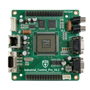
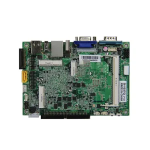
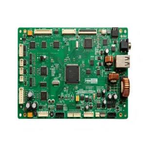
Explore our top-tier turnkey assembly modules validated across enterprise networking, consumer smart devices, industrial automation, and green energy controllers.
In modern product lifecycle management (PLM), rapid hardware iteration is no longer a luxury—it is the core bottleneck or catalyst for global technology leadership.
Consumer electronics, industrial IoT nodes, and automotive sub-assemblies now face replacement cycles under 12 months. Design verification test (DVT) cycles that previously spanned quarters must now conclude within weeks to preserve market dominance.
The ubiquity of Edge AI, Wi-Fi 7, 5G NR, and compact sensors requires micro-via HDI boards (1+N+1 to arbitrary layer), high-Tg substrates, and tight impedance matching tolerances (±7%) even during preliminary prototype stages.
Enterprise procurement teams avoid locked single-source dependencies by employing prototype specialists capable of immediately validating multi-sourced pin-compatible active/passive components across real production parameters.
Shenzhen's Greater Bay Area houses an unmatched electronics supply chain ecosystem where raw materials, chemical processes, precision tooling, and high-speed SMT assembly merge in one geographic cluster.
Direct proximity to Huaqiangbei and tier-one franchise distributors allows procurement of hard-to-find passives, high-density connectors, and active ICs within 60 minutes, bypassing days of overseas parcel transit.
Fully compliant, modern green industrial parks host dedicated surface finish lines capable of delivering high-uniformity ENIG, ENEPIG, Immersion Silver, and Immersion Tin under rigid environmental ISO 14001 governance.
Over 50 in-house CAM and DFM specialists scrutinize aperture sizes, aspect ratios, thermal reliefs, and copper balances within 2 hours of file drop, neutralizing assembly defects before physical copper is etched.
Every fast-turn work order features unique QR/barcode routing. Real-time Shop Floor Control (SFC) enables transparent traceability down to the solder paste lot, reflow profile timestamp, and technician ID.
Engineering Fact: Prototyping in an integrated Shenzhen EMS ecosystem reduces design-to-validation latency by up to 65% compared to fragmented western assembly models that outsource bare board fabrication to offshore brokers while attempting local assembly.
Precision parameters governed under certified IPC-A-600 Class 2/3 bare board fabrication and IPC-A-610 Class 2/3 electronic assembly standards.
| Capability Parameter | Standard Prototype Range | Advanced / Precision Limits | Quality Standard |
|---|---|---|---|
| Layer Count | 1 to 16 Layers | Up to 32 Layers (Blind/Buried, HDI) | IPC-6012 Class 3 |
| Min Trace / Spacing | 3.5 mil / 3.5 mil (0.09mm) | 2.5 mil / 2.5 mil (0.063mm) | IPC-A-600 |
| Min Mechanical Drill | 0.20 mm (8 mil) | 0.15 mm (6 mil) | Automated CNC X-Ray Drill |
| Laser Micro-Via Drill | 0.10 mm (4 mil) | 0.075 mm (3 mil) UV Laser | HDI Any-Layer Stackup |
| SMT Chip Component Placement | 0201 packages, SOT, SOP, QFP | 01005 passives & 0.3mm pitch QFN | IPC-A-610 Class 3 |
| Fine-Pitch BGA Placement | Pitch ≥ 0.40 mm | Pitch ≥ 0.30 mm, CSP, PoP (Package-on-Package) | 3D X-Ray Void < 10% |
| Surface Finishes | HASL Lead-Free, Standard ENIG | ENEPIG, Immersion Ag/Sn, Hard Gold 50u" | RoHS & REACH Compliant |
| Turnaround Fast-Track | 24-48 Hours (2-4 Layers) | 72 Hours (6-8 Layers Quick-Turn) | Expedited Priority Line |
From automotive powertrain sub-units to life-critical medical imaging instrumentation, fast prototyping demands rigorous sector-specific compliance from day one.
Rapid validation of multi-core processing architectures, radar processing PCBA, and high-voltage Battery Management Systems (BMS). Built within our strict IATF 16949 certified production environment to eliminate field vulnerability early.
Certified under ISO 13485, our rapid prototype workflow supports non-invasive diagnostic boards, digital X-ray processing systems, and patient monitoring devices where thermal stability and extreme low-noise design are non-negotiable.
Heavy duty motor drivers, crane control interfaces, and environmental particle monitors demand assemblies resistant to mechanical vibration, severe ESD, and wide ambient temperature swings (-40°C to +125°C).
Emerging engineering imperatives reshaping the quick-turn PCBA landscape through 2030 and how forward-looking manufacturers adapt.
Manual engineering review is augmented with neural net algorithms that verify Gerber gerber clearances, solder mask slivers, and component footprints in real-time, cutting the RFQ-to-cam pipeline down to minutes.
To support micro-miniaturized wearables and ultra-compact Edge AI trackers, prototypes increasingly embed thin-film resistors and capacitive layers directly within core substrates to free vital top/bottom surface area.
Regulatory scrutiny around PFAS, carbon footprints, and hazardous effluent requires clean closed-loop wastewater reclamation, halogen-free laminates, and low-temperature bismuth-tin alloy soldering developments.
Advanced EMS providers construct full mechanical and thermal digital twins before assembly, predicting reflow warpage on complex mixed-thickness hybrid PCB panels before physical heat exposure occurs.
When global buyers qualify a China PCB prototyping manufacturer, they demand more than speed. They require institutional rigor across 5 core governance pillars.
Comprehensive Non-Disclosure Agreements (NDAs) signed prior to file sharing, coupled with strict internal network partitioning and encrypted file access logs for all proprietary gerbers and firmware.
Zero tolerance for counterfeit components. Direct franchise procurement via Arrow, Avnet, Digi-Key, Mouser, and verified original semiconductor makers backed by factory Certificates of Conformance (CoC).
The engineering team fine-tuning the 5-board prototype must seamlessly scale the setup into a 100,000-unit batch on the same SMT lines, eliminating re-qualification risks and tooling redesign overheads.
100% Automated Optical Inspection (AOI), 3D X-Ray Inspection (AXI) for BGA/QFN hidden joints, solder paste inspection (SPI), First Article Inspection (FAI), and customized functional testing (FCT).
Real-time automated milestone updates via ERP, customs pre-clearance documents, export packaging compliant with anti-static standards (ESD MIL-STD-1686), and priority door-to-door global express shipping.
Direct, engineering-level answers regarding rapid prototype cycle times, DFM procedures, assembly tolerances, and global shipping logistics.
For double-sided standard FR-4 bare boards, expedited production takes as little as 24 hours. 4 to 8-layer rigid boards can be fabricated in 48 to 72 hours. When paired with turnkey quick-turn SMT assembly, fully assembled and inspected PCBA prototypes are routinely completed within 3 to 7 working days, subject to component availability.
We require RS-274X Gerber files (or ODB++ archive) including layer stackup details, a comprehensive Bill of Materials (BOM) detailing exact Manufacturer Part Numbers (MPN) and authorized alternates, a Pick-and-Place (Centroid / XY data) file, and explicit assembly/testing instructions.
No. STHL operates an absolute No-MOQ policy. We happily manufacture and assemble prototype quantities from 1 to 5 boards for engineering validation, proofs of concept (PoC), and academic R&D, allowing seamless scaling into high-volume manufacturing later on.
We employ inline high-resolution 3D X-Ray Inspection (AXI) calibrated to detect solder bridge formation, excess solder balling, head-in-pillow defects, and voiding percentages across hidden leadless pads, guaranteeing that BGA voiding levels stay well below IPC-A-610 Class 3 limits (<15%).
Yes. Our component engineering staff analyzes supply chain lead-times immediately upon RFQ submission. If a part has extended lead times or is End-of-Life (EOL), our engineers propose functionally equivalent, pin-compatible alternates with verified parametric cross-references for client sign-off.
We execute binding bilateral Non-Disclosure Agreements (NDAs) prior to project review. Design data is stored within an isolated, role-restricted ERP/MES ecosystem. We strictly prohibit external sharing of customer design collateral, schematics, and embedded binaries under severe compliance audit protocols.
Explore our specialized assemblies engineered for mission-critical environmental monitoring, automotive ADAS, power management, and industrial machinery.