Explore production-grade printed PCB assemblies manufactured with rigorous IPC Class 2/3 quality controls across telecommunications, automotive electronics, and environmental telemetry.
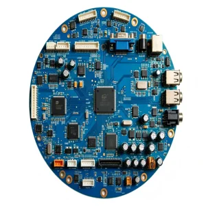

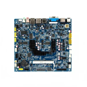
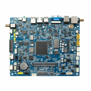

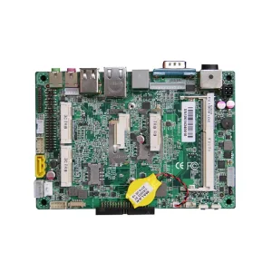
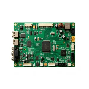
How China's premier PCB manufacturers have transformed from low-cost board fabricators into technologically advanced, vertically integrated engineering powerhouses delivering IPC Class 3 mission-critical assemblies.
The global printed circuit board industry accounts for over $85 billion in commercial value. While regional initiatives like the US CHIPS Act and European Chips Act seek to rebuild domestic capacity, more than 52% of the world's complex multilayer rigid, flexible, and High-Density Interconnect (HDI) boards originate within mainland China. Modern procurement directors recognize that decoupling from China is functionally prohibitive due to unparalleled supply chain depth, ultra-fast NPI tooling, and component colocation.
Modern telematics, AI accelerator hardware, and edge computing demand sub-3mil line width and space (L/S), high-layer counts (up to 32+ layers), and extreme thermal dissipation. STHL leverages modified semi-additive processes (mSAP), blind/buried microvias via CO2/UV laser drilling, and advanced high-Tg substrates (FR-4 High-Tg 170°C+, Rogers, Taconic, and Nelco) to mitigate dielectric loss and ensure signal integrity above 28 Gbps per lane.
Traditional procurement splits bare board fabrication, active component procurement, and SMT assembly across three disjointed vendors. This fragmented workflow induces finger-pointing during assembly failures, solder mask misalignment, or thermal profile delamination. STHL provides a unified turnkey framework: DFM review, bare board fab, authorized component procurement, SMT/THT assembly, and functional box-build testing under a single accountable quality management system.
Shenzhen’s Bao'an district offers unmatched microelectronics cluster density, enabling rapid turn-around, instant component availability, and robust manufacturing fail-safes.
Situated in Shenzhen's prime industrial corridor, STHL has real-time access to raw copper laminates, specialty chemical prepregs, solder pastes, custom aluminum extrusions, and passive packaging within a two-hour transit window. This geographic agglomeration slashes prototype NPI cycle times from typical European or North American timelines of 4–6 weeks down to 3–5 working days without sacrificing QA checks.
With an active inventory catalog of over 500,000 components and direct accounts with top global distributors including Arrow Electronics, Avnet, Digi-Key, Mouser, Farnell, and Future Electronics, STHL eliminates counterfeit risks. Incoming parts undergo stringent lot-level inspection, decapsulation sampling, and XRF analysis before warehouse allocation, maintaining unbroken lot traceability back to original semiconductor fabs.
High-mix low-volume (HMLV) orders often suffer punitive surcharges or outright refusal at massive tier-1 EMS conglomerates. Conversely, micro-shops lack automotive or medical credentials. STHL bridges this chasm with 7 automated SMT lines and 2 THT lines, executing 5-board prototype validations on identical production machinery, feeders, and reflow ovens used for 100,000+ unit mass production runs.
Comprehensive engineering limits, dimensional tolerances, and multi-tier surface finish capabilities supporting mission-critical commercial and industrial designs.
| Fabrication Parameter | Standard Prototype Capability | Advanced HDI / Mass Production | Inspection & Verification Protocol |
|---|---|---|---|
| Layer Count & Stackup | 1 – 8 Layers (FR-4 High-Tg) | Up to 32 Layers (Rigid, Flex, Rigid-Flex) | Cross-section microsectioning & X-ray lamination check |
| Min Trace Width / Space (L/S) | 3.5 mil / 3.5 mil (0.088mm) | 2.5 mil / 2.5 mil (0.063mm, mSAP ready) | Automated Optical Inspection (AOI) with CAM comparators |
| Min Laser Drilled Microvia | 0.10mm (4 mil) UV/CO2 Laser | 0.075mm (3 mil) Staggered & Stacked Via-in-Pad | 3D X-Ray Inspection (AXI) & copper plating fullness >95% |
| SMT Placement Pitch | 0.4mm Pitch QFP / 0.5mm BGA | 0.3mm Ultra-Fine BGA, CSP & 01005 passives | Koh Young 3D Solder Paste Inspection (SPI) & inline AOI |
| Surface Finishes | Lead-Free HASL, OSP | ENIG, ENEPIG, Immersion Silver, Hard Gold 30u" | XRF plating thickness testing & solderability dipping |
| Impedance Control | ±10% Single-ended / Differential | ±5% Ultra-tight Controlled Impedance (TDR) | Polar CITS8800 Controlled Impedance Test System |
| Thermal Management Core | Standard Aluminum 1.0–2.0 W/m.K | Copper Core, Ceramic, Heavy Copper (up to 12oz) | Thermal cycling (-40°C to +150°C) & high-pot insulation |
Engineered for hostile operating environments: How our China-manufactured printed PCBs power certified systems worldwide.
Compliant with rigorous IATF 16949 standards, our in-vehicle communication and Battery Management System (BMS) PCBA solutions endure persistent mechanical vibration, wide temperature swings (-40°C to +125°C), and chemical exposure. High-copper traces dissipate thermal loads in traction inverters, while conformal coatings insulate high-voltage traces against dielectric breakdown.
From smart blood glucose monitors to infusion drug delivery pumps and clinical patient telematics, medical hardware requires zero-defect manufacturing. Fabricated under ISO 13485 cleanroom controls, our assemblies feature bio-compatible finishes, thorough ionic contamination testing, and persistent lot-level firmware flashing with full device serialization.
Wastewater monitoring stations, exhaust gas sensors, and smart grid automation hardware demand decades of uninterrupted field reliability. Our heavy-copper, high-Tg circuit boards feature transient voltage suppression, optical galvanic isolation, and potted mechanical enclosures, resisting sulfurization and corrosive atmospheric elements.
How our Shenzhen facility safeguards overseas engineering files, enforces zero-defect quality systems, and guarantees international regulatory compliance.
Prior to receiving any Gerber, schematic, or BOM data, STHL executes legally binding Non-Disclosure Agreements governed under international legal jurisdictions. Internal engineering networks employ air-gapped CAM workstations, role-based permission servers, and encrypted storage. Firmware injection stations run on local closed networks with automatic binary wiping to prevent IP exfiltration.
Every single PCB is etched with an indivisible 2D DataMatrix code. Our Manufacturing Execution System (MES) links each board directly to specific solder paste lots, pick-and-place nozzle feeds, reflow thermal chamber logs, AOI/AXI optical scans, and individual test operators. If a field discrepancy arises, complete genealogy reports can be queried within seconds.
STHL maintains audited quality certifications: IATF 16949 (Automotive), ISO 13485 (Medical Devices), ISO 9001 (Quality Management), and ISO 14001 (Environmental Management). Finished assemblies comply with EU RoHS, REACH, and UL 94V-0 flammability ratings, backed by formal CoC (Certificate of Conformance) documentation in every shipping carton.
Addressing the convergence of micro-pitch semiconductor packaging and bare printed circuit board fabrication.
As smart devices condense silicon footprints, classic subtractive etching hits physical limits below 30µm trace width. STHL’s technical roadmap integrates semi-additive process (SAP/mSAP) methodologies, bridging conventional HDI with IC carrier packaging substrates. Additionally, embedding passive capacitors and thin-film resistors directly into inner dielectric laminates frees outer layer surface area by up to 28%.
Conventional 2D AOI generates excessive false-call rates on micro-features. STHL is actively deploying deep-learning computer vision models trained across millions of reflow solder joint variations. This intelligent inspection stack distinguishes harmless cosmetic flux shadows from genuine micro-voids, bridge hazards, and tombstoning, achieving post-reflow defect rates under 15 PPM.
Environmental compliance is rapidly shifting toward life-cycle emissions accountability. Our production roadmap incorporates zero-halogen high-Tg core substrates, low-temperature bismuth-tin (Sn-Bi) solder alloys to reduce reflow thermal energy consumption by 35%, and closed-loop wastewater recycling systems that reclaim 92% of etching water inside our PCB wet-processing centers.
Technical clarity on file formats, lead-time acceleration, component validation, and logistics guarantees.
Explore specialized industrial, consumer, and wireless PCB assemblies built to stringent IPC-A-610 Class 3 workmanship criteria.
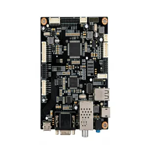
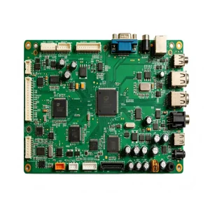

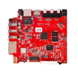
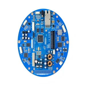
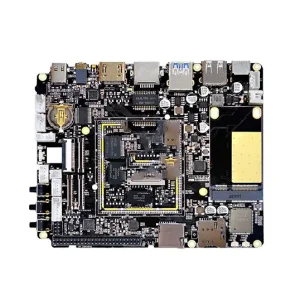
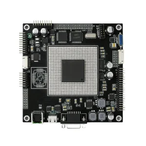
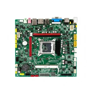
Send your Gerber files and BOM today. Our 50+ process engineers will return a complimentary, confidential Design-for-Manufacturability (DFM) review and comprehensive turnkey quotation within 24 hours.
