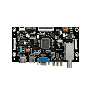
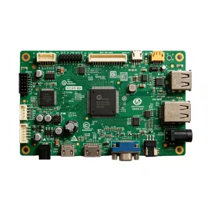
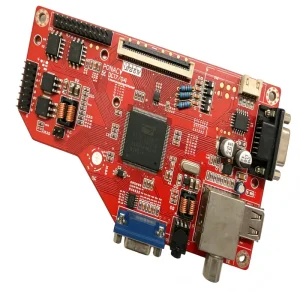
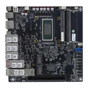
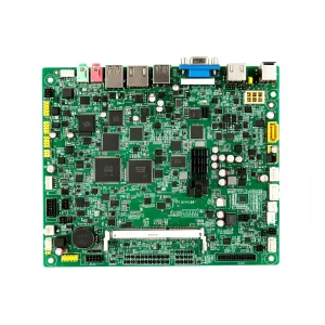
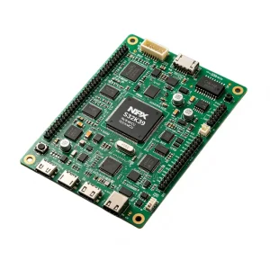
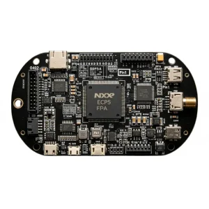
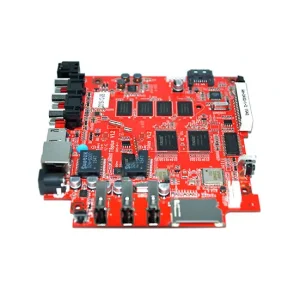
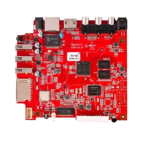
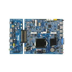
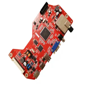
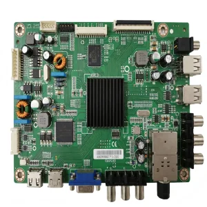
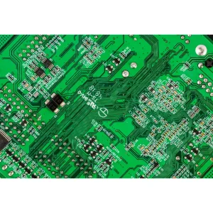
Explore our high-reliability, micro-pitch SMT assembly solutions engineered across smart photonics, embedded edge computing, power monitoring, and industrial automotive systems.
In modern electronic hardware development, the convergence of component miniaturization, multi-gigahertz signal frequencies, and relentless time-to-market demands has completely transformed the role of the surface mount device (SMD) manufacturing partner.
The industry migration toward 0201, 01005, and 03015 passive packages, alongside 0.3mm micro-pitch Ball Grid Arrays (BGA) and Wafer-Level Chip-Scale Packaging (WLCSP), eliminates traditional solder margins. High-speed placement requires closed-loop optical alignment, laser coplanarity verification, and sub-micron positioning repeatability.
IPC-7351B StandardSegmenting PCB layout, bare board fabrication, active BOM procurement, SMT placement, and enclosure assembly across multiple disparate vendors introduces substantial hand-off risks, logistics bottlenecks, and quality finger-pointing. True turnkey EMS consolidates accountability under a single comprehensive ERP/MES pipeline.
End-to-End GovernanceHigh-power switching transistors (GaN, SiC) and dense compute modules require specialized thermal dissipation architectures, including heavy-copper PCBs, aluminum cores, and thermal via arrays. Ensuring zero solder voiding underneath critical thermal pads demands precise solder paste rheology and inert atmosphere reflow control.
Vacuum & N2 SolderingShenzhen STHL Electronics Co., Ltd. operates a 10,000+ m² dust-free, ESD-protected facility in Bao'an, Shenzhen. Our smart workshop integrates 7 automated SMT lines, 2 THT/DIP lines, 2 dedicated functional test lines, and 2 complete box-build integration lines.
| Manufacturing Dimension | Technical Specification & Capability | Industrial Quality Standard |
|---|---|---|
| SMD Component Capability | Passives down to 01005 (0402 metric); fine-pitch QFP/QFN to 0.3mm pitch; BGA/uBGA down to 0.25mm ball pitch; POP (Package on Package) | IPC-A-610 Class 2 & Class 3 |
| SMT Line Configuration | High-speed modular pick-and-place systems (Yamaha, Panasonic); automatic stencil printers with 2D/3D paste inspection; 10-zone reflow with Nitrogen (N2) atmosphere | Placement accuracy ±0.03mm (3 sigma) |
| Automated Inspection | Inline 3D Solder Paste Inspection (SPI); Multi-angle inline 3D Automated Optical Inspection (AOI); Offline High-Resolution X-ray Inspection (AXI) for BGA/QFN voiding | BGA Void Ratio < 10% (IPC-7095 Standard) |
| PCB Substrate Diversity | FR-4 (Standard, High-Tg, Halogen-Free), Aluminum Core (MCPCB), Copper Core, Rogers High Frequency, Ceramic, Polyimide Flex, Rigid-Flex, HDI up to 32 layers | UL 94V-0 Certified Flammability |
| THT / DIP Capabilities | Lead-free wave soldering, selective wave soldering for mixed-technology PCBA, automated axial/radial lead insertion, manual assembly work cells | RoHS 3 (EU 2015/863) & REACH Compliant |
| System Integration & Box Build | Custom wire harness termination, robotic conformal coating, silicone/polyurethane potting, ultrasonic plastic welding, final mechanical assembly, custom blister packaging | Full lot-level MES traceability |
Procuring semiconductor components in a volatile geopolitical and market climate requires deep upstream relationships and rigorous incoming inspection. Operating from the core of Shenzhen's electronics ecosystem enables STHL to mitigate supply chain disruptions with localized inventory networks and immediate direct-factory access.
We maintain an active network of over 100 franchised distributors and vetted direct manufacturers—including Arrow, Avnet, Digi-Key, Mouser, STMicroelectronics, Microchip, and TDK—covering over 500,000 verifiable part numbers. Every single reel entering our facility undergoes comprehensive incoming material qualification (IQC), including decapsulation testing, X-ray leadframe inspection, and pin solderability analysis to safeguard against counterfeit or reclaimed silicon.
Independent third-party audits ensure our production protocols comply with stringent aerospace, automotive, medical, and commercial industry regulations.
Automotive Quality Management System certified. Rigorous adherence to Advanced Product Quality Planning (APQP), Production Part Approval Process (PPAP Level 3), FMEA defect prevention, and 8D corrective actions for mission-critical automotive electronics.
Automotive Tier-1 & Tier-2Medical Device Quality Management Standard. Controlled cleanroom environments, electrostatic discharge (ESD) protection to ANSI/ESD S20.20, and complete Device Master Records (DMR) / Device History Records (DHR) ensuring full clinical lifecycle accountability.
Medical Diagnostic GradeFoundational quality management system across engineering, procurement, surface mount assembly, through-hole insertion, and customer service. Real-time statistical process control (SPC) and CPK tracking across all high-speed production assets.
Standard Industrial BaselineEnvironmental Management Certification guaranteeing sustainable manufacturing. Closed-loop chemical recovery, lead-free solder paste utilization (SAC305), halogen-free laminate options, and strict compliance with EU RoHS 3 and REACH SVHC directives.
Green ManufacturingFrom precision agricultural grow systems to renewable power generation and industrial vision nodes, our SMD manufacturing lines are configured to meet rigorous operational tolerances.
High-efficiency LED grow luminaires require heavy-copper metal-core PCBs (MCPCB) capable of continuous high-amperage operation. Our automated lines apply optimized thermal paste stencils and void-free reflow profiles to prevent hotspot formation, preserving high lumen output and extending diode operational life past 50,000 hours.
Thermal Dissipation MasteryPhotovoltaic power converters and smart micro-inverters demand extreme thermal cycle resilience and high dielectric isolation. We utilize high-Tg FR-4 combined with selective conformal coating to safeguard sensitive MCU and gate-driver traces against outdoor humidity, salt spray, and extreme temperature fluctuations (-40°C to +85°C).
High Voltage Creepage ControlIn aerospace VHF Omnidirectional Range (VOR) receivers and high-frequency communication modules, signal integrity and parasitic capacitance must be tightly controlled. Our production lines integrate controlled-impedance PCB routing validation, RF shielding solder cages, and automated 3D optical coplanarity checks to eliminate RF phase distortion.
RF Signal IntegrityAs electronic packages continue to shrink while power densities climb, our engineering laboratories are actively deploying next-generation assembly processes to stay ahead of the microelectronics curve.
Engineering pilot lines are already validating ultra-miniaturized 008004 (0201 metric) components using nanotech electroformed stencils, specialized Type 6 ultra-fine solder pastes, and customized high-magnification vision nozzles. This level of miniaturization unlocks unprecedented packaging densities for next-gen wearables and biomedical implants.
Roadmap Horizon 2026-2027For mission-critical power electronics and dense BGA/QFN arrays, traditional convection reflow can leave small air entrapments. Vacuum-assisted vapor phase soldering eliminates oxidation and drives solder joint voiding below 3%, maximizing thermal conductivity and vibration resilience in extreme operating environments.
Ultra-Low VoidingBy interfacing 3D SPI paste volume inspection directly with our automatic stencil printers, real-time offset corrections are calculated and applied automatically without human intervention. Similarly, post-reflow 3D AOI data loops back to pick-and-place feeders to immediately catch micro-drifts before defects occur.
Industry 4.0 Closed-LoopIn-depth technical answers addressing Design for Manufacturability (DFM), quality tolerances, component procurement integrity, and overseas shipping protocols.
To initiate an engineering DFM and formal cost quotation, our engineering team requires: (1) Gerber files in RS-274X or ODB++ format showing copper layers, solder mask, and drill details; (2) Bill of Materials (BOM) in Excel with exact Manufacturer Part Numbers (MPN), descriptions, references, and approved vendor lists; (3) Pick-and-place (Centroid/XY) coordinate data; and (4) Assembly drawings outlining conformal coating keep-out zones and custom testing criteria.
We purchase components solely through authorized global distribution agreements (Digi-Key, Mouser, Arrow, Avnet) and verified direct silicon manufacturers. Every shipment undergoes rigorous Incoming Quality Control (IQC) containing barcode traceability, anti-static verification, moisture sensitivity level checks (J-STD-033), packaging verification, and sample decapsulation or XRF elemental analysis whenever supply chain anomalies arise.
We do not enforce any Minimum Order Quantity (No MOQ). Our production infrastructure is tailored to support clients across their entire product lifecycle—from rapid 24-hour quick-turn NPI prototypes (1 to 5 boards) to pilot runs (50 to 500 units), all the way up to high-volume multi-hundred-thousand batch mass manufacturing on the exact same certified lines.
Hidden solder joints are inspected using automated high-resolution 3D X-ray Inspection (AXI). This system measures solder volume, calculates ball sphericity, identifies micro-bridging or open circuits, and verifies that intermetallic voiding stays safely below 10%, fully adhering to IPC-7095 Class 3 criteria for high-reliability assemblies.
IP protection is structured around strict legal and physical firewalls. We execute enforceable bilateral Non-Disclosure Agreements (NDAs) prior to receiving any design files. Internally, customer Gerber data and proprietary firmware images are hosted on isolated, encrypted servers with tiered role-based access. Firmware flashing occurs in secured work cells equipped with tamper-proof audit trails.
Yes. Our component engineering division performs comprehensive BOM health assessments. We identify obsolete (EOL), single-sourced, or long-lead items and propose footprint-compatible second-source alternatives or localized Chinese direct-factory equivalents that can yield 15% to 30% unit cost reductions while preserving identical pinouts and electrical characteristics.
We operate two dedicated testing lines equipped for: (1) In-Circuit Testing (ICT) using custom bed-of-nails fixtures; (2) Flying Probe testing for quick-turn prototypes without fixture NRE; (3) Functional Circuit Testing (FCT) validating digital I/O, analog signals, RF power, and sensor response; and (4) Environmental Stress Screening (ESS) encompassing thermal cycling and burn-in chambers.
STHL routinely exports to over 90 countries—including the United States, Germany, the United Kingdom, Italy, Poland, Japan, South Korea, and Australia. We offer flexible Incoterms including EXW, FOB Shenzhen/Hong Kong, CIF, and DDP (Delivered Duty Paid), collaborating directly with leading freight express carriers (DHL, FedEx, UPS, air/ocean cargo) to guarantee safe transit.
Explore specialized surface-mount assemblies configured for precision safety equipment, telemetry, environmental monitoring, smart automation, and wireless infrastructure.
Send your Gerber files, BOM, and assembly drawings today. Our engineering department will perform a complimentary Design for Manufacturability (DFM) review and deliver a complete turnkey quotation within 24 hours.