
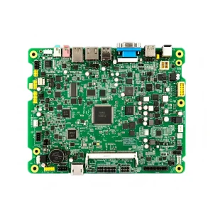
Explore our surface mount technology assemblies deployed across telecommunications, renewable energy converters, life-science instrumentation, and advanced automation.

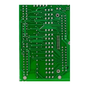
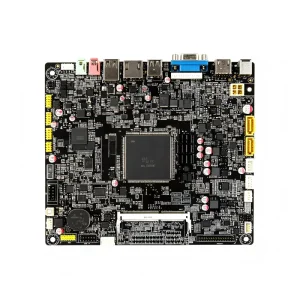
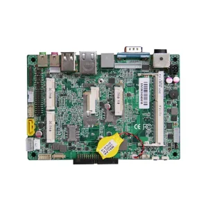

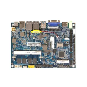
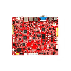
From 01005 ultra-miniature passive passives to 0.3mm ultra-fine pitch Ball Grid Arrays (BGA), Shenzhen STHL Electronics leverages modular dual-lane pick-and-place systems and nitrogen-inert vacuum reflow soldering to conquer microelectronics assembly challenges.
Modern telecommunications, biomedical sensors, and smart IoT devices demand extreme volumetric efficiency. Our modular high-speed mounters support chip sizes down to 01005 (0.4mm × 0.2mm) and 03015 metric with an absolute component placement accuracy of ±0.025mm at Cpk ≥ 1.33.
Equipped with dual-nozzle intelligent vision recognition, electronic feeder feedback loops, and micro-tension substrate clamping, our production lines eliminate tombstoning, skewing, and bridging under dense packaging constraints.
Processing high-density integrated circuits such as Ball Grid Arrays (BGA), Chip Scale Packaging (CSP), and Quad Flat No-Lead (QFN) devices with pitch intervals down to 0.3mm requires meticulous thermal and solder volume control.
We deploy nano-coated electroformed stencils, laser direct structuring, and multi-zone heating profiles that ensure equalized surface tension, zero voiding (<8% voiding ratio surpassing IPC-A-610 Class 3 specifications), and superior shear strength across all solder joints.
Zero-defect production begins with Closed-Loop Quality Architecture. Before reflow, 3D Solder Paste Inspection (SPI) dynamically verifies paste height, volume, coplanarity, and area coverage down to 1μm resolution.
Post-reflow quality verification combines telecentric multi-angle 3D Automated Optical Inspection (AOI) with 130kV High-Resolution Automated 3D X-Ray Inspection (AXI), revealing internal head-in-pillow (HIP) defects, solder balling, micro-voids, and substrate micro-fractures in concealed terminals.
| SMT Engineering Parameter | Production Capability & Tolerance Limit | Inspection Protocol & Quality Standard |
|---|---|---|
| Smallest Component Handling | 01005 (0.4 × 0.2mm), 0201, 0402, 0603, Micro-QFN, 0.3mm pitch BGA | IPC-A-610 Class 3 Optical Vision Feeder Calibration |
| Placement Accuracy & Repeatability | ±0.025mm (Chip), ±0.035mm (QFP / IC), Cpk ≥ 1.33 | Closed-Loop Optical Linear Encoders + Real-Time Vision |
| Substrate Dimensions (Min / Max) | 50mm × 50mm up to 610mm × 1200mm (Ultra-long LED & Industrial) | Multi-Point Vacuum Clamping & Anti-Warp Support Tooling |
| Reflow Soldering Environment | 10-Zone Forced Air Convection + N2 (Nitrogen Inert, O2 < 500ppm) | KIC Thermal Profiler 24-Channel Real-Time Thermocouple Mapping |
| BGA Voiding Ratio Control | Void Area < 8% across all array balls (Standard allows up to 25%) | 3D Computed Tomography / High-Penetration AXI Non-Destructive |
| Supported Substrate Materials | FR-4 (High Tg 170-180°C), Polyimide Flex, Rigid-Flex, Aluminum, Ceramic, Rogers | IPC-6012 & IPC-6013 Verification with Cross-Section Microsectioning |
From mission-critical automotive powertrain electronics to life-sustaining medical diagnostic systems, our SMT manufacturing lines strictly align with the highest regulatory and functional benchmarks.
Automotive electronics require zero-ppm escape rates. We implement complete APQP, FMEA, and PPAP Level 3 documentation for Engine Control Units (ECUs), Battery Management Systems (BMS), ADAS radar sensors, and smart cockpit controllers.
Automated conformal coating, potting, and harsh-vibration screening guarantee thermal-cycling resistance from -40°C to +125°C under operating load conditions.
Deploying assemblies for vital-sign patient monitors, ultrasonic transducers, hemodialysis controllers, and in-vitro diagnostics requires sterile process hygiene and rigorous trace records.
STHL maintains a Class 100,000 cleanroom assembly environment, component lot serialization, complete Device Master Records (DMR), and Device History Records (DHR) conforming to FDA and MDR audit requirements.
Programmable Logic Controllers (PLCs), high-voltage DC-DC converters, dynamic servo drives, and DIN-rail power switches demand elevated dielectric breakdown protection and immunity against heavy EMI.
We apply high-Tg FR-4 bases, heavy copper tracks (up to 4oz), specialized selective soldering for high-power magnetic inductors, and 100% automated electrical Hi-Pot burn-in testing.
Solar inverters, maximum power point tracking (MPPT) optimizers, and wind turbine blade pitch controllers face continuous outdoor exposure, UV exposure, and thermal shock.
We execute multi-layer automated silicone and polyurethane conformal coating, nitrogen-inert soldering, and accelerated environmental stress screening (HASS/HALT) to guarantee a 25-year design service lifetime.
Positioned in the heart of Shenzhen’s world-renowned hardware silicon valley (Bao'an District), STHL harnesses the most concentrated microelectronics supply cluster on Earth to provide unmatched turnaround velocity, component authenticity, and line agility.
Our centralized procurement division maintains direct accounts and API integrations with top global distributors including Arrow Electronics, Avnet, Digi-Key, Mouser, Farnell, and Future Electronics, supplemented by certified tier-1 domestic semiconductor fab partners.
Every active reel is verified through incoming barcode logging, de-capping verification, and X-ray counter audits, eliminating counterfeit components and ensuring full BOM traceability.
Every single PCB assembly passing through our 10,000+ m² workshop receives a unique laser-engraved 2D DataMatrix code. Our Manufacturing Execution System (MES) continuously logs solder paste lot numbers, reflow temperature profiles, mounter feeder locations, and automated test logs.
Should any anomaly arise 5 years down the line, our clients can audit the exact feeder, operator, machine, and environmental conditions present during fabrication.
Component obsolescence and unexpected price surges can stall entire production runs. Our dedicated hardware component engineering division actively monitors lifecycle stages (EOL, LTB, NRND).
We provide drop-in pin-compatible alternative suggestions with complete parametric data, thermal comparisons, and pre-compliance test reports—consistently achieving 15% to 35% BOM cost savings without sacrificing board reliability.
Seamless transition from prototype validation to high-volume manufacturing hinges on upfront engineering rigor. Our preliminary Design for Manufacturing review prevents costly re-spins and line delays before fabrication ever begins.
Upon receiving your Gerber RS-274X, ODB++, or IPC-2581 files, our 50+ engineering team executes automated multi-rule audits. We verify pad-to-trace clearance, solder mask dam width (min 0.075mm), copper balance across internal signal layers, and thermal relief web width on ground planes.
Addressing pad geometry mismatches prevents solder bridging, tombstoning, and copper delamination during multi-cycle reflow operations.
We analyze component-to-component spatial clearances, pick-and-place fiducial positioning, conveyor edge clearances (5mm standard), and tall component shading effects across the reflow thermal curve.
By standardizing panelization schemas with V-scoring or mouse-bite breakaways, we maximize SMT feeder utilization and eliminate manual post-assembly solder touch-ups.
A reliable circuit board is only as good as its verifiable test coverage. We collaborate with OEM engineering teams to integrate dedicated test pads (minimum 0.8mm diameter with 1.27mm center-to-center pitch) across critical power and signal nets.
STHL designs and builds custom pneumatic In-Circuit Test (ICT) fixtures, bed-of-nails functional testers (FCT), flying probe test arrays, and automated flashing rigs for MCU firmware deployment.
Exporting to European, North American, and Asia-Pacific markets requires strict adherence to international environmental, electrical safety, and material declarations. STHL guarantees 100% compliant shipments backed by third-party testing.
All surface mount assembly processes utilize lead-free solder alloys (SAC305, SAC0307, or SN100C) strictly complying with EU Directive 2011/65/EU (RoHS 3) and Regulation (EC) No 1907/2006 (REACH SVHC). Certified ICP material lab test reports accompany all production lots.
Every bare PCB substrate is sourced from certified raw laminate manufacturers (Shengyi, ITEQ, Rogers, Isola) bearing official Underwriters Laboratories (UL) yellow card stamps. Full flame retardancy rating UL 94V-0 ensures fire safety across consumer, automotive, and industrial applications.
Our certified IPC trainers and production operators inspect all electronic assemblies according to IPC-A-610 (Acceptability of Electronic Assemblies) and IPC-J-STD-001 (Requirements for Soldered Electrical and Electronic Assemblies). Dedicated lines support Class 3 high-reliability mission-critical requirements.
We understand that firmware, gerber plots, and schematic blueprints are core intellectual properties. We execute enforceable Non-Disclosure Agreements (NDAs) prior to project review. All internal design repositories are protected by multi-tier encryption, isolated VLANs, and biometric cleanroom access controls.
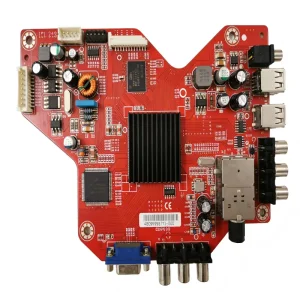
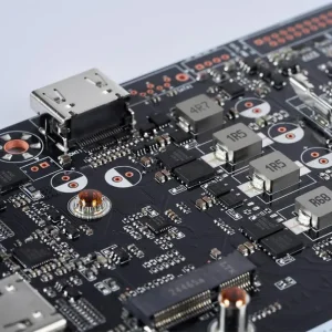
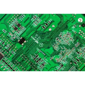
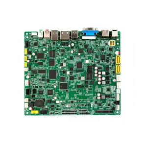
Explore our high-voltage conversion, communication, mission-critical avionic alerts, and industrial sensor PCBA products manufactured with zero-defect standards.
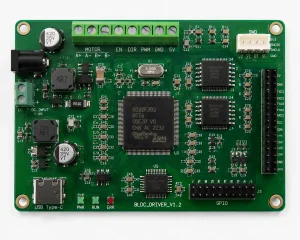
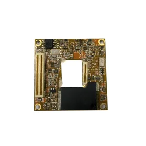
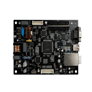
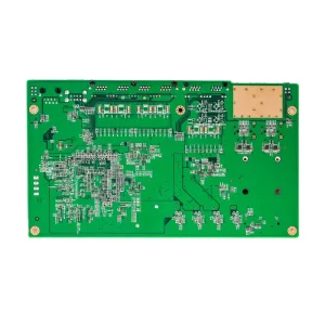
Comprehensive engineering and commercial responses designed for technical directors, hardware supply managers, and overseas purchasing executives qualifying a Chinese EMS partner.
STHL operates with no minimum order quantity (No MOQ). We maintain dedicated agile quick-turn prototype SMT lines designed for batches from 1 to 50 units for engineering verification test (EVT) and design verification test (DVT), scaling seamlessly to mass production runs exceeding 500,000 units on high-speed dual-lane lines.
We source directly from authorized franchise distributors (Arrow, Avnet, DigiKey, Mouser) and original component manufacturers (OCMs). All incoming material undergoes rigorous inbound verification including lot code checks, moisture barrier bag (MBB) validation, packaging anti-static verification, microscope marking inspection, and optional X-ray die analysis.
To provide a formal DFM analysis and turnkey quotation within 24 to 48 hours, we require: (1) RS-274X or ODB++ Gerber files, (2) Machine Pick-and-Place Centroid (.xy / .txt) coordinates, (3) Bill of Materials (BOM) detailing manufacturer part numbers (MPNs), package footprints, and reference designators, and (4) Test Specifications/Requirements.
For quick-turn SMT prototypes with components readily available in domestic stock, turnaround is as swift as 3 to 5 business days. Standard turnkey prototype production averages 10 to 15 business days. Scheduled high-volume production orders are delivered according to rolling forecast pull-signals, Kanban agreements, or consignment stocking buffers.
Because hidden leads cannot be inspected using 2D optical cameras, we deploy 100% 3D Automated X-ray Inspection (AXI) on all BGA, LGA, and QFN assemblies. AXI measures solder ball coplanarity, circularity, bridging, cold solder crystallization, and void percentages to ensure complete compliance with IPC-A-610 Class 3 standards.
Yes. Beyond surface mount assembly, STHL offers comprehensive Box Build and Higher Level Assembly (HLA) services. This includes precision CNC and plastic injection enclosure sourcing, silicone gaskets, custom wire harness integration, ultrasonic welding, laser serial marking, final packaging, and direct pallet dropshipping worldwide.
Submit your Gerber files and BOM today to receive a comprehensive Design for Manufacturability (DFM) assessment, cost-down component analysis, and formal transparent quotation within 24 hours.