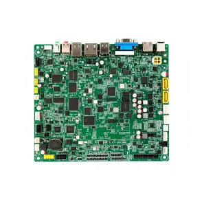
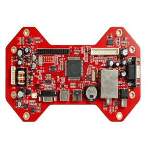
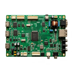
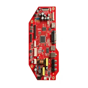
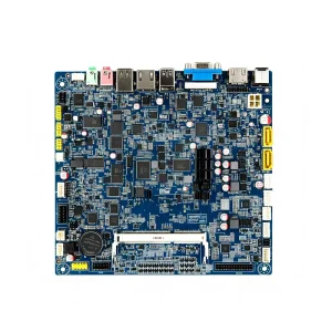
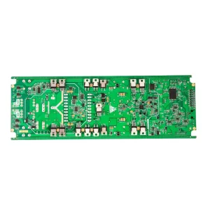
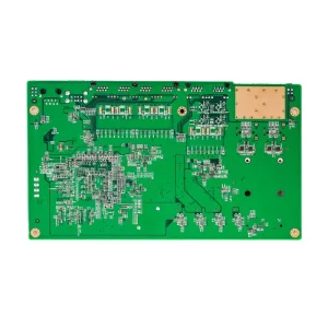
STHL combines high-speed SMT assembly with multi-angle 3D AOI inspection algorithms to ensure zero-defect escape across critical clean-energy, industrial, and medical systems.
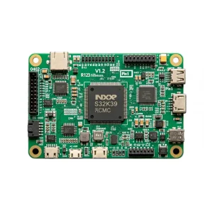
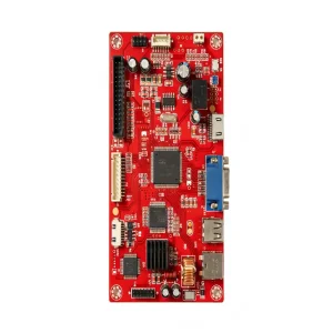
Modern Surface Mount Technology (SMT) demands micro-geometric precision. As component packaging shrinks below 0201 metric footprints, traditional two-dimensional color extraction is obsolete.
Unlike planar camera systems susceptible to PCB warpage shadows and optical reflections, true 3D AOI projects structured fringe moiré light patterns. This enables complete height-map calculation across solder joints, evaluating precise solder fillet heights, wetting angles, and coplanarity down to 1 µm resolution.
Traditional AOI systems suffer from high False Call Rates (FCR), creating costly operator fatigue and unverified overrides. Modern AI engines utilize deep convolutional neural networks (CNNs) trained on millions of micro-defect classifications to distinguish harmless flux halos from real electrical bridging.
AOI serves as the brain of modern surface-mount lines. By linking post-reflow 3D AOI and 3D SPI (Solder Paste Inspection) directly to the automatic screen printer and chip shooter via CFX/Hermes protocols, real-time machine offset adjustments occur autonomously before defective boards can form.
Evaluating a PCBA manufacturing partner requires looking past superficial equipment lists. Global procurement directors and lead hardware engineers must audit how automated optical inspection is integrated into production to prevent costly field recalls.
| Procurement Dilemma | Factory Floor Failure Mechanism | STHL Standardised AOI Engineering Remedy |
|---|---|---|
| High Escape Rates vs. High False Calls | Uncalibrated 2D optical systems force operators to loosen tolerances to prevent assembly line bottlenecking, causing cold joints, lifted leads, and voids to escape into finished inventory. | Implementation of Koh Young 3D AOI & AI-assisted defect classifiers. Multi-directional digital projection captures real joint volume, ensuring genuine solder bridging is caught while reducing false alarms below 0.15%. |
| Component Miniaturization & Shadowing | Tightly packed 0201/01005 passives placed adjacent to large inductors, shielded RF cans, or connectors suffer from light shadowing, rendering 2D camera images unreadable. | STHL uses multi-angle structured blue-light moiré fringe projection with 4 to 8 side-view cameras. Shadow-free height mapping detects coplanarity deviations down to 1 µm across dense RF and high-speed layouts. |
| High-Mix Low-Volume (HMLV) Setup Lag | Traditional AOI programming takes hours or days per revision. Low-volume engineering builds are often skipped from full inspection, introducing significant prototype risks. | Integrated auto-programming software with direct CAD/Gerber centroid extraction. Our production team establishes validated IPC Class 3 inspection recipes in under 45 minutes, ensuring 100% inspection even for pilot batches of 5 units. |
| Audit Traceability & Liability Defense | When an electronic module fails in the field, generic pass/fail logs lack the visual proof needed to diagnose root causes or defend against warranty claims. | Full-spectrum MES 1-to-1 barcode logging. Every serialized PCBA retains high-resolution 3D volumetric images, reflow temperature profiles, and component lot numbers for over 10 years to support rigorous automotive and medical audits. |
Optical inspection parameters must align with industry-specific failure modes. STHL configures dedicated AOI inspection libraries tailored to specialized operating environments.
IATF 16949-compliant inspection focused on structural joint integrity for on-board chargers, BMS, and ADAS ECUs subjected to continuous shock, vibration, and thermal cycling.
ISO 13485-governed quality protocols safeguarding life-critical patient monitors, infusion pumps, and surgical tools from microscopic electrical leakage.
Specialized for photovoltaic inverters, wind power controllers, and smart meters operating in harsh outdoor environments over 15 to 25-year service lifespans.
Ensuring ultra-high signal integrity and mechanical stability for robotic neural cores, industrial PLCs, and rugged networking gateways exposed to electromagnetic interference.
Quality is not inspected into a product; it is built into the process. STHL embeds inline inspection gates at every phase of the surface-mount and through-hole production lines.
100% paste volume, height, area, and offset measurement. Stencil cleaning triggers automatically upon volumetric paste deviations.
Verifies missing components, polarity misalignments, bill-of-materials matching, and skew before permanent thermal bonding.
Continuous thermocouple tracking ensuring thermal ramp-up, liquidus dwell time, and cooling gradients match solder alloy specs.
12-way phase moiré measurement for solder fillets, tombstoning, wetting angles, lifted leads, and micro-bridging.
Non-destructive volumetric analysis for BGA, QFN, and bottom-terminated components, measuring void ratios below 15%.
Custom bed-of-nails fixture testing, power-up diagnostics, boundary scan, and firmware flashing under simulated loads.
Cross-border hardware manufacturing demands ironclad intellectual property safeguards, strict hazardous substance controls, and responsive engineering communication across time zones.
Our 10,000+ m² facility operates under auditable quality management systems verified by independent third-party registrars, guaranteeing systematic process control from incoming material to final shipment packaging.
Every raw bare board, passive component, active IC, and solder chemistry procured by STHL comes with verifiable Certificate of Compliance (CoC) documentation, ensuring seamless customs clearance globally.
We bridge the communication gap between Western engineering centers and Shenzhen manufacturing hubs. Dedicated bilingual project engineers provide 24-hour turnaround on technical queries and DFM audits.
As advanced packaging, System-in-Package (SiP), and flexible hybrid electronics reshape circuit board topology, optical inspection technologies must evolve to maintain automated quality assurance.
By leveraging synthetic training models, next-generation AOI engines will generate thousands of virtual defect iterations (e.g., subtle dewetting, lifted leads, micro-bridging) from pristine CAD models, eliminating the need to wait for physical production line faults before calibrating AI vision systems.
Consolidating surface optical inspection and planar X-ray computed tomography into a single synchronized dual-lane system. This integration allows simultaneous measurement of exterior surface solder wetting and hidden internal micro-voids across BGA and QFN balls at line speed.
Direct integration between AOI quality telemetry and the virtual plant twin. Real-time solder fillet measurement drift automatically triggers fine micro-adjustments in reflow oven temperature profiles, eliminating thermal deviations caused by seasonal ambient temperature shifts.
Actionable answers to the common technical and procurement dilemmas encountered when evaluating turnkey electronics assembly partners.
2D AOI relies on flat optical photographs and color segmentation to infer solder geometry. It struggles with PCB warpage, shadows from tall components, and specular reflection off shiny lead-free solder. 3D AOI projects structured phase-shift moiré fringe light to calculate the actual height (Z-axis) of each solder joint, measuring fillet volume, lifted leads, and coplanarity quantitatively against IPC-A-610 Class 3 specifications.
No. 3D AOI inspects the exterior surface geometry of solder joints (such as gull-wing leads, chip terminations, and through-hole barrels). Hidden joints beneath packages like BGAs, LGAs, and QFN ground pads cannot be seen optically. High-reliability manufacturing requires a combined testing approach: 3D AOI for surface joints and 3D AXI to detect internal solder voids, bridging, and head-in-pillow defects under package bodies.
We deploy deep-learning AI vision filters integrated with our Koh Young 3D inspection algorithms. Rather than relying on manual operator overrides which risk missing true defects, our AI models review flagged anomalies against thousands of verified good/bad joint libraries. This keeps our False Call Rate below 0.15% while guaranteeing zero solder-bridge escapes across small-batch engineering prototypes.
To program both 3D SPI and 3D AOI lines, we require standard ODB++ data or RS-274X Gerber files (including copper, paste, silkscreen, and soldermask layers), an XY Centroid (Pick-and-Place) file containing component reference designators, X/Y coordinates, and component rotation angles, alongside a detailed BOM listing exact manufacturer part numbers.
Over 60% of SMT soldering defects stem from poor paste deposition. STHL's inline 3D SPI directly measures solder paste height, area, volume, and bridge proximity right after stencil printing. If paste volume drops below 75% or exceeds 130%, the SPI system signals an alarm and automatically communicates with the screen printer to pause and trigger an automatic stencil wipe before parts are placed.
Every printed circuit board passing through our facility receives a laser-etched 2D DataMatrix barcode. As it moves through SMT lines, its serial number is linked to complete 3D height maps, optical inspection images, SPI volume records, reflow oven thermal curves, and incoming component reel lot numbers within our MES database, archived for up to 10 years.
Send us your Gerber files and Bill of Materials (BOM) today for an engineering review, comprehensive DFM feedback, and a turnkey PCBA manufacturing quotation.
From complex multi-layer automotive autopilot modules and intelligent robotic controllers to consumer smart devices, our automated manufacturing ensures exceptional solder joint reliability.