Explore our validated reference designs and turnkey assembled modules manufactured to strict IPC-A-610 Class 3 and IATF 16949 standards.

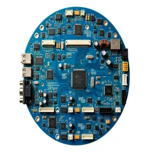

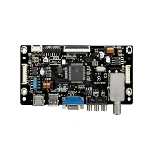
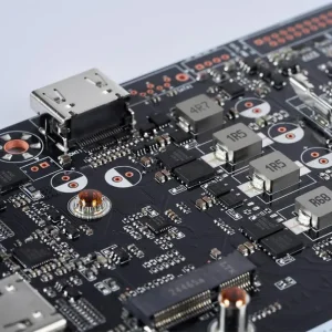
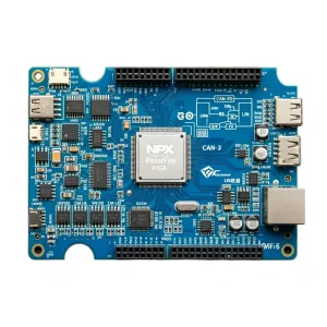
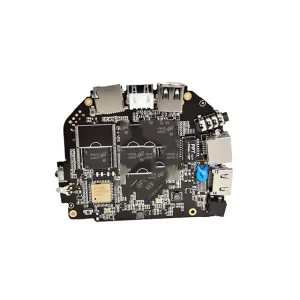
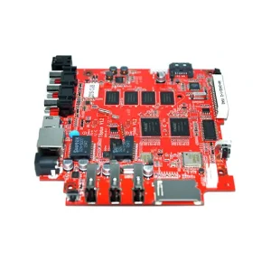
The electronics manufacturing services (EMS) sector is undergoing structural change driven by embedded AI, miniaturization, and supply ecosystem demands.
Global demand for edge-computing and smart IoT has accelerated component packaging down to 01005 passives and ultra-fine-pitch BGAs (0.35mm pitch). Standard contract manufacturing is no longer sufficient; Tier-1 OEMs require integrated micro-electronics engineering capable of handling complex layer stack-ups and signal integrity.
With electrification and Advanced Driver Assistance Systems (ADAS), electronic stability control (ESP) and transmission control units (TCU) demand functional validation under extreme thermal cycling. The industry standard has transitioned toward IPC Class 3 and zero-defect automotive protocols (IATF 16949).
Fragmenting supply networks across separate bare-board fabricators, overseas brokers, and regional assemblers creates costly lead times and engineering handoff defects. Modern procurement strategies prioritize one-stop partners who control everything from DFM review to automated conformal coating.
Shenzhen's industrial cluster provides hardware developers and enterprise buyers with unprecedented supply velocity, component depth, and scaling efficiency.
| Manufacturing Dimension | Fragmented Multi-Vendor Sourcing | STHL Turnkey Shenzhen Ecosystem |
|---|---|---|
| Component Procurement Lead Time | 6–14 weeks due to multiple regional distributors and shipping hand-offs. | 3–7 business days leveraging deep access to 100+ vetted regional suppliers and central stock. |
| DFM & Engineering Resolution | Iterative delays; 5–8 days back-and-forth between PCB fab and SMT plant. | Under 24 hours; unified engineering team executes layout, tooling, and panelization checks. |
| Quality Traceability & Risk | High vendor finger-pointing between bare-board defects and assembly errors. | Unified MES Tracking; end-to-end audit trails from bare laminate to functional tester. |
| NPI to Mass Production Velocity | Requires multiple re-toolings across different facilities; 3–6 months. | Seamless ramp-up on identical automated SMT lines with 0 Minimum Order Quantity (MOQ). |
Turnkey PCBA solutions adapted to real-world industrial environments, regional certification codes, and demanding operational conditions.
In utility-scale solar farms across North America and Southern Europe, high-power inverters operate in harsh high-temperature conditions. Our heavy copper PCB fabrication (3oz–6oz) and automated conformal coating provide long-term dielectric stability, protecting against humidity, dust ingress, and thermal degradation.
For European Tier-1 automotive assemblies including Electronic Stability Programs (ESP) and Transmission Control Units (TCU), assemblies must withstand harsh road vibration. We employ multi-axis 3D AOI, real-time X-ray inspection, and underfill dispensing to deliver high solder joint reliability across automotive temperature ratings (-40°C to +125°C).
Portable patient telemetry and hospital diagnostics deployed across Japan and the EU require strict baseline shielding and cleanroom assembly. Fabricated under ISO 13485 clean conditions, boards undergo high-potential insulation testing and micro-BGA placement to ensure clinical reliability.
How we safeguard cross-border procurement through strict intellectual property management and audited international compliance.
We execute strict bilateral NDAs prior to handling Gerber files, firmware binaries, or BOM architecture. Our internal cloud ERP enforces compartmentalized data access, ensuring your proprietary schematics and intellectual property remain protected throughout the production cycle.
Full manufacturing alignment with European and global standards: RoHS 3.0 (EU 2015/863), REACH (EC 1907/2006), and WEEE compliance. Solder pastes and wash chemistries are fully documented with analytical testing reports, guaranteeing smooth customs clearance.
Dedicated technical program managers support design reviews during North American and European business hours. Our engineers provide proactive BOM obsolescence warnings and suggest equivalent replacements for hard-to-find components.
Our engineering investments are aligned with the next generation of industrial and commercial electronics assembly.
1-to-3 stage laser micro-via drilling, 0.35mm pitch BGA placement, automated 3D SPI and inline 3D AOI closed-loop feedback systems.
Active nitrogen-reflow environments, specialized thin stencils, and ultra-accurate vacuum pick-up tooling for dense IoT and wearable devices.
Deep-learning algorithmic defect classification on automated optical inspection, predictive maintenance on SMT feeders, and real-time solder paste monitoring.
Embedding passive and active dies directly into PCB inner layers to support thermal dissipation and high-speed data transmission for advanced computing.
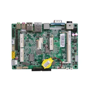
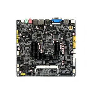
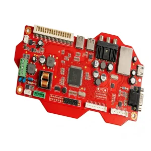
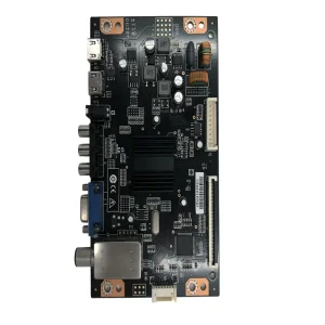
Explore additional high-performance assemblies manufactured across our 7 automated SMT lines and dedicated functional test cells.



Key technical and operational questions answered by our manufacturing engineering and procurement teams.
