Engineered to satisfy stringent electromagnetic compliance, thermal dissipation, and industrial reliability criteria across mission-critical infrastructure.
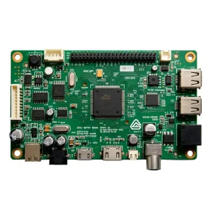
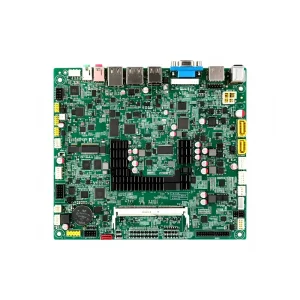
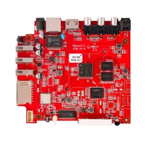
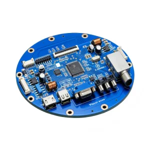

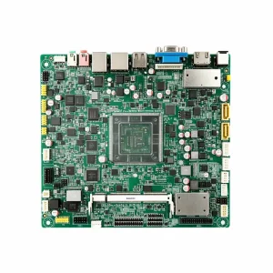
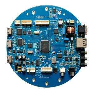
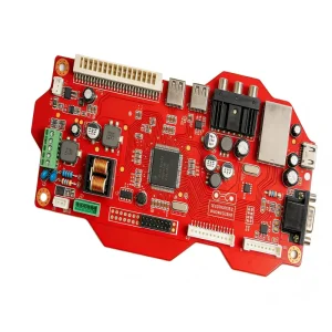
Navigating the convergence of sub-millimeter component miniaturization, thermal density challenges, and multinational supply chain resilience in modern contract electronics manufacturing.
Modern hardware architectures demand 01005 (0402 metric) passive placement, 0.3mm pitch fine-ball array packages (FBGA), and micro-via High-Density Interconnects (HDI Any-Layer). Manufacturers must deploy advanced multi-axis optical alignment and 3D solder paste inspection (3D SPI) to ensure zero coplanarity faults and solder bridging under dense packaging parameters.
The proliferation of automotive EV powertrains and high-voltage energy storage systems requires robust dielectric breakdown prevention and low-loss laminate substrates (Rogers, Megtron, Teflon, Polyimide). Controlled impedance routing (single-ended and differential pair tolerances within ±5%) is rigorously validated through Time Domain Reflectometry (TDR).
With persistent component obsolescence and counterfeit IC infiltration, premier PCB assembly manufacturers rely on authorized franchise distributors (Arrow, Avnet, DigiKey, Mouser) backed by incoming X-ray fluorescence (XRF) material verification, de-capsulation testing, and ERP-integrated serial lot tracking from raw bare board to final boxed device.
The global electronics manufacturing services (EMS) marketplace has matured beyond simple cost-arbitrage labor. Modern original equipment manufacturers (OEMs), Tier-1 automotive integrators, and industrial medical device creators require integrated engineering ecosystems where design-for-manufacturability (DFM), bare circuit fabrication, active silicon sourcing, and automated testing converge in real time. Dividing fabrication across regional silos generates logistical latency, mismatched tooling tolerances, conflicting quality accountability, and amplified freight expenses.
Operating out of Bao'an, Shenzhen—the epicenter of the worldwide electronics component supply network—STHL Electronics delivers an uncompromised turnkey pipeline. By marrying direct localized access to 500,000+ authorized electronic parts with internal engineering validation under IPC-A-610 Class 2 and Class 3 guidelines, our partners eliminate production bottlenecks before stencil laser-cutting commences. This comprehensive transparency translates into compressed new product introduction (NPI) cycles and ironclad quality guarantees.
Empirical hardware tolerances and machinery benchmarks calibrated for high-yield surface mount (SMT), plated through-hole (THT), and electro-mechanical box build.
| Parameter / Metric | Standard Capability Profile | Advanced / Aerospace / Medical Limits |
|---|---|---|
| Layer Count & Stackup | 1 to 32 Layers (FR-4, High-Tg, Aluminum) | Up to 48 Layers; Rigid-Flex & Any-Layer HDI (1+N+1 to 4+N+4) |
| SMT Component Range | 0201 passives, QFP, SOP, SOT, QFN, DFN | 01005 chips, 0.3mm pitch micro-BGA, PoP (Package on Package) |
| SMT Placement Accuracy | ±0.035mm (Cpk ≥ 1.33) at 45,000 cph per line | ±0.025mm laser alignment with real-time coplanarity check |
| Board Dimensions | Min: 50mm × 50mm | Max: 510mm × 460mm | Ultra-thin: 0.2mm flex | Max board length up to 1200mm (LED) |
| PCB Surface Finishes | HASL lead-free, ENIG (Electroless Nickel Immersion Gold) | Immersion Silver, OSP, ENEPIG, Hard Gold Finger plating |
| Reflow Soldering Environment | 10-Zone Forced Air Convection (Lead-Free SAC305/Sn96.5Ag3.0Cu0.5) | Nitrogen (N2) atmosphere reflow, residual O2 < 50 ppm |
| Quality Inspection Technology | Online 3D SPI, Inline 3D AOI (Koh Young), Manual QC | 3D Computed Tomography (CT) X-Ray, Flying Probe, ICT, Boundary Scan |
| Conformal Coating & Potting | Selective spray coating (Acrylic, Silicone, Polyurethane) | Automated robotic dispensing with UV-cure inspection fluorescent dye |
| Compliance Governance | RoHS, REACH, WEEE, Conflict Minerals Declaration | IPC-A-610 Class 3, ISO 13485:2016, IATF 16949:2016, UL 94V-0 |
Algorithmic verification of pad geometries, solder mask clearances, pin 1 polarities, and component lifecycle (EOL/NRND) before fabrication.
Procurement via direct semiconductor makers and franchise channels with lot-code validation, MSL moisture barrier verification, and ESD storage.
Laser stencil printing, solder paste height 3D verification, dual-gantry high-speed component shooting, and profiled multi-zone reflow.
3D AOI for tombstoning, solder bridging, and missing parts; high-voltage oblique X-ray to inspect BGA solder ball collapse and voiding ratios.
Precision manual component insertion followed by nitrogen-assisted selective wave soldering to safeguard neighboring SMT components.
Automated IC flashing, bed-of-nails ICT, boundary-scan testing, and custom hardware simulation under operating loads.
Automated conformal coating against humidity and corrosive atmospheres, thermal potting, ultrasonic welding, and cable harness pinning.
Mechanical chassis assembly, final retail carton packaging, drop testing, and expedited direct dispatch across North America, Europe, and Asia.
Mitigating legal, functional, and intellectual liabilities through accredited certifications, bilingual technical program management, and rigorous legal frameworks.
Proprietary schematics, Gerber archives, microcontroller firmware binaries, and algorithmic formulas are safeguarded by internationally binding bilateral Non-Disclosure Agreements. Production files reside within an isolated, role-based network infrastructure with encrypted repositories and zero unauthorized exterior access.
Full compliance with global regulatory dictates: European Union RoHS 3 (Directive 2015/863) restricting hazardous chemicals, REACH SVHC substance tracing, and Dodd-Frank Act conflict mineral declarations (3TG: Tantalum, Tin, Tungsten, Gold). Every bare PCB and solder flux batch includes verified mill test and safety data sheets.
Eliminating timezone friction and communication gaps. Our 50+ staff engineering division offers fluent English technical advisory for real-time Design for Assembly (DFA) resolution, rapid alternate component recommendation during market shortages, and transparent engineering change orders (ECO) directly synced with client systems.
Total Quality Management across engineering, SMT, and testing pipelines.

Automotive electronics certification; zero-defect failure prevention.

Sterile and high-risk medical device board fabrication & tracking.
Sustainable, eco-conscious industrial chemical handling and disposal.
Customized PCBA engineering matching operational environments—from subsea sensors and flight-deck avionics to smart power grids and Class II/III medical devices.
Applications: Battery Management Systems (BMS), On-Board Chargers (OBC), Head-Up Displays (HUD), ADAS millimeter-wave radar sensors, and Supplemental Restraint Systems (SRS).
Engineering Criteria: High vibration resistance, AEC-Q100/Q200 component qualifications, thermal cycling endurance from -40°C to +125°C, and underfill stabilization on heavy silicon dies.
Applications: Multiparameter patient monitors, portable ultrasound devices, infusion pump controllers, and digital diagnostic x-ray controllers.
Engineering Criteria: Low-leakage currents adhering to IEC 60601-1 safety margins, bio-compatible conformal finishes, ultra-clean board wash protocols, and complete DHR (Device History Record) archival.
Applications: Fly-by-Wire (FBW) flight computers, Inertial Measurement Units (IMU), terrain mapping radars, and multifunction cockpit instruments (MFD).
Engineering Criteria: IPC-A-610 Class 3 / Space Addendum assembly, extensive staking and ruggedized mechanical potting, anti-vibration staking, and thermal shock testing across altitude gradients.
Applications: Heavy electric crane controllers, SCADA telemetry nodes, high-torque motor drives, programmable logic controllers (PLC), and security perimeter units.
Engineering Criteria: Heavy copper traces capable of conducting 50A+ sustained currents, galvanic isolation between power and logic planes, and thick polyurethane conformal layers resisting industrial chemicals.
Applications: Solar string inverters, grid Load Balancers, rack-mount Power Distribution Units (PDU), and commercial battery energy storage containers (BESS).
Engineering Criteria: High-creepage and clearance design validation, partial discharge prevention at 1500VDC, and long-life electrolytic capacitors rated for 105°C continuous duties.
Applications: Enterprise load balancing appliances, commercial tablets, embedded Linux gateways, and automated smart access transmitters.
Engineering Criteria: Low insertion-loss dielectric laminates, DDR4/DDR5 high-speed memory timing synchronization, 5G/Wi-Fi 6E RF impedance matching, and back-drilled via stubs to minimize signal attenuation.
How our advanced fabrication facilities are transforming electronic packaging through artificial intelligence, embedded passive components, and zero-carbon cleanrooms.
Traditional design reviews are transitioning toward neural-network analysis. Our deep-learning automated optical inspection (AOI) models analyze hundreds of thousands of solder joint images to discern real defects from minor cosmetic variations, reducing false-call rates by 70% while improving true defect detection down to single-digit PPM levels.
To surmount surface real-estate limitations, we are deploying advanced substrate embedding where discrete resistors, capacitors, and active silicon dice are integrated directly within interior prepreg layers. This eliminates stray inductances, improves RF transmission characteristics beyond 40 GHz, and reduces board surface area by up to 40%.
Aligned with global carbon neutrality benchmarks, our facility integrates closed-loop wastewater filtration for chemical wash processes, solar-supplemented SMT thermal ovens, and low-temperature bismuth-tin (Sn-Bi) soldering alloys that lower reflow thermal spikes from 245°C to 170°C, drastically curbing embodied manufacturing emissions.
Evaluated and trusted by engineering executives, hardware architects, and supply chain managers spanning North America, Western Europe, and Asia-Pacific.
"Excellent team to work with and fast delivery with high-quality boards. We are very happy to work with such a good supplier. Thanks again."

"Please extend my thanks to your team for the hard work in preparing these samples. This experience has strengthened my confidence in your company, and I look forward to discussing bulk orders soon."

"We are satisfied with the last order. You did a great job on those boards and the lead time was short. I will place a new order soon."

"The order was perfect—exactly as specified, with top quality. Highly recommend this reliable supplier."

"Very fast delivery, professional supplier and professional product. We will place a new order very soon!"

"We have tested all the boards and I am highly pleased. I will repeat my order soon. Thank you again for your excellent service."

Essential clarifications for hardware engineering leads, NPI program managers, and strategic supply chain directors evaluating manufacturing partners.
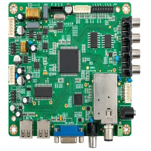
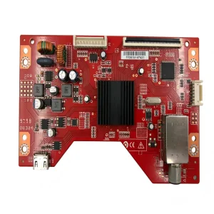
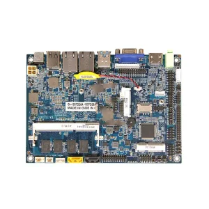
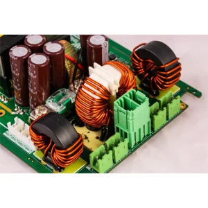
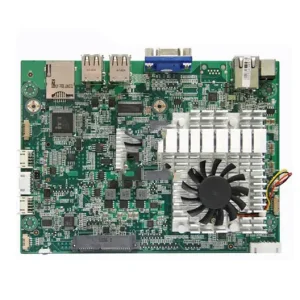
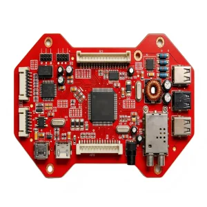
Featured sub-assemblies demonstrating high-power conversion, precision navigation, avionics control, and vehicular human-machine interfaces.


Submit your Gerber archives, pick-and-place files, and Bill of Materials today for an NDA-protected, comprehensive Design for Manufacturability (DFM) assessment and detailed turnkey cost evaluation.
