Verified hardware platforms engineered across medical diagnostics, renewable power grids, telecommunication hubs, and enterprise IoT infrastructures.
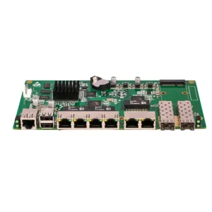
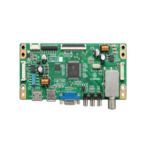
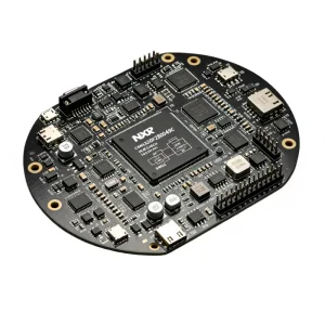
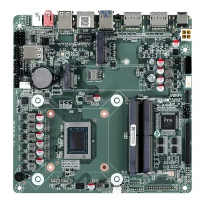
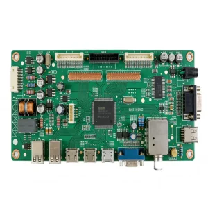
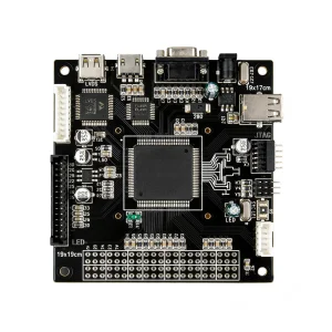
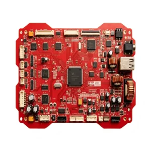
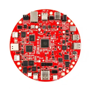
Bridging the structural gap between rapid component obsolescence, high-density interconnections (HDI), and predictable global commercial scalability.
The global landscape for printed circuit board assembly (PCBA) has transformed from isolated contract manufacturing into deeply integrated Turnkey Electronics Manufacturing Services (EMS) ecosystems. As modern embedded systems demand smaller form factors, heightened thermal efficiency, and multi-gigahertz signal integrity, the margin for fabrication and assembly deviations has dropped to near zero. OEMs in North America, the European Union, and Asia-Pacific no longer view PCBA factories as mere soldering workshops; they are strategic technological partners tasked with managing supply chain volatility, component authenticity, Design for Manufacturability (DFM) verification, and lifecycle sustainability.
Current industrial metrics reveal that over 70% of electronics hardware revisions fail during the first pilot run not because of schematic design flaws, but due to assembly mismatch—such as inadequate solder paste volume repeatability, solder bridge short-circuits under fine-pitch Ball Grid Arrays (BGAs), or component stress induced by thermal reflow profiling. Consequently, top-tier global enterprises are consolidating their manufacturing partnerships, migrating away from fractured broker networks toward accredited, end-to-end facilities capable of handling high-mix, low-to-high volume cycles under rigorous international standards such as IPC-A-610 Class 3, ISO 13485, and IATF 16949.
While discussions of regional reshoring remain prevalent, the core physical dependencies of active silicon, passive capacitors, and specialized substrates continue to rely heavily on concentrated industrial clusters. Fragmented multi-vendor sourcing models introduce compounding transit delays, multi-tier freight markups, and disjointed quality liabilities.
The rapid proliferation of IoT sensors, Edge-AI processing units, and high-frequency communication modules has accelerated the standard adoption of 01005 passives, 0.3mm pitch micro-BGAs, and Quad Flat No-Lead (QFN) packages. These geometries require sub-micron precision mounting and real-time closed-loop optical control.
Geopolitical turbulence and component supply bottlenecks have caused a surge in grey-market broker activity. Enterprise procurement requires AS6081 and IDEA-STD-1010 compliant component authentication, lot-level ERP tracking, and non-destructive automated X-ray inspection (AXI) to guarantee authenticity.
Analyzing the compound velocity, rapid prototyping cycles, and localized supply chain density that define modern Chinese turnkey PCBA manufacturing.
Shenzhen, often hailed as the world's electronics hardware capital, represents an unmatched industrial synergy that cannot be replicated by simply assembling discrete machines under one roof. At our Bao'an manufacturing campus, Shenzhen STHL Electronics operates directly within a 1-hour supply chain perimeter that encompasses bare board fabrication, authorized franchised semiconductor distribution, custom sheet metal stamping, precision tooling, cable harness braiding, and automated injection molding.
Where traditional Western or fragmented offshore facilities expend weeks coordinating bare PCB delivery, waiting for passive component consolidations, and handling cross-border customs declarations for raw materials, an integrated Shenzhen factory transitions from approved engineering Gerbers to full Surface Mount Technology (SMT) production in as little as 24 to 48 hours for rapid prototypes, and 5 to 7 days for complex turnkey NPI (New Product Introduction) runs.
| Evaluation Parameter | Fragmented Multi-Vendor Approach | Shenzhen Turnkey Tier-1 Factory (STHL Standard) | Operational Engineering Benefit |
|---|---|---|---|
| NPI Prototyping Lead Time | 3 to 6 Weeks (Multiple vendor hand-offs) | 24 to 72 Hours (Direct line allocation) | Accelerates time-to-market by up to 75% for venture-backed hardware and medical device pilots. |
| BOM Component Sourcing | Split between catalog brokers & overseas distributors | Franchised direct tier-1 distribution + 500k+ in-stock lines | Eliminates counterfeit risks; guarantees volume wholesale tier pricing. |
| Engineering Change Orders (ECO) | Protracted renegotiation, freight delays, re-tooling fees | Real-time internal DFM/DFA engineering adjustments | Seamless iteration updates directly within MES/ERP before stencil laser cut. |
| Quality Accountability | Finger-pointing between bare-board fab and assembly shop | Single-point end-to-end institutional warranty | Total root-cause analysis (8D Reports) handled under one quality management team. |
| Inspection Infrastructure | Manual visual check or basic offline 2D AOI | Inline 3D SPI + Multi-angle 3D AOI + High-resolution 3D AXI | Sub-micron defect detection prevents latent solder fractures and field failures. |
This operational velocity does not sacrifice standard compliance. Shenzhen's mature industrial ecosystem has evolved far beyond rudimentary assembly: it is governed by enterprise Enterprise Resource Planning (ERP) integrations, modern Manufacturing Execution Systems (MES), and automated line cleanrooms maintaining strict ISO Class 8 ESD environments under ANSI/ESD S20.20 protocols.
How component selection, substrate thermal conductivity, and conformal encapsulation directly dictate field longevity in severe operational environments.
In life-support ventilators, digital radiography systems, and clinical monitoring devices, PCBA failures can be catastrophic. Production is anchored in our ISO 13485 cleanroom lines. We enforce Class 3 electronic solder joints, biocompatible conformal coatings (Parylene/Polyurethane), strict moisture-barrier packaging, and 100% functional in-circuit testing (ICT) to eliminate latent field anomalies.
Operating under IATF 16949 certification, automotive assemblies require zero-defect tolerances under continuous thermal cycling (-40°C to +125°C) and violent mechanical vibrations. SMT lines incorporate nitrogen-purged reflow chambers to minimize solder joint voiding under power transistors and micro-controllers to less than 10%, well beyond standard consumer thresholds.
High-voltage battery management systems (BMS) and utility-scale solar inverter PCBAs process extreme electrical currents. These designs deploy heavy copper boards (3oz to 6oz), specialized FR4 high-Tg (Tg 170°C+) laminates, and aluminum substrates to ensure rapid thermal dissipation, combined with automated selective soldering for high-amperage terminal blocks.
Air Data Inertial Reference Units and avionics navigation platforms demand uncompromising trace precision, controlled characteristic impedance (±5%), and gold-surface finishes (ENIG / ENEPIG). Every solder batch undergoes full radiographic automated X-ray analysis to inspect hidden BGA ball intermetallic connections.
Industrial networking infrastructure requires multi-layer designs (up to 32+ layers) running multi-gigabit data interfaces. These assemblies utilize low-loss materials (Rogers, Megtron), ultra-tight component spacing, and specialized press-fit connector installations tested via multi-channel automated functional jigs.
Wastewater monitoring apparatus, toxic gas detectors, and outdoor industrial telemetry equipment face persistent chemical exposure, moisture condensation, and corrosive atmospheres. We apply precision robotic selective spray conformal coatings and silicone encapsulations validated by thermal shock testing.
A step-by-step technical framework utilized by Chief Procurement Officers and VP-level Hardware Engineering teams to separate Tier-1 EMS leaders from intermediate brokers.
For international enterprise buyers, qualifying a printed circuit board assembly partner involves far more than comparing quotation unit prices on a spreadsheet. In an era marked by complex silicon packaging, component allocations, and stringent liability regulations, an inadequate assembly partner represents an enterprise risk that can result in total product recalls, lost market windows, and brand damage. Engineering leaders look for verified evidence across four core technical pillars:
Does the factory maintain a dedicated engineering team capable of conducting Valor-grade automated DFM analyses before cutting stencils? A tier-1 factory analyzes thermal relief sizing, component copper-clearance, shadow effects during wave soldering, and bill-of-materials lifecycle risks (EOL/NRND) immediately upon RFQ submission.
Leading EMS factories operate high-speed Yamaha and Panasonic modular pick-and-place lines integrated with 3D Solder Paste Inspection (SPI) directly networked to the stencil printer. If solder volume deposition shifts beyond ±10%, the system halts the printer automatically, eliminating over 85% of soldering defects before reflow.
Does the plant feature high-resolution 3D Automated Optical Inspection (AOI) alongside transmission X-ray (AXI) for BGA, QFN, and package-on-package (PoP) assemblies? High-quality assembly requires calculating solder ball void percentages, wetting angles, and package coplanarity across 100% of critical parts.
Each PCBA panel should feature laser-etched 2D data matrix codes. Our MES records the exact reel lot number, SMT machine feeder slot, solder paste jar batch number, operator identity, reflow thermal profile, and automated test log for every single circuit board produced, archived for over 10 years.
Enterprise clients require strict non-disclosure protections. We implement strict digital firewalls, isolated offline programming cells for proprietary firmware flashes, and comprehensive Non-Disclosure Agreements (NDAs) executed prior to any file transmission.
Moving beyond bare boards, global enterprises increasingly demand finished-device integration: ultrasonic plastic welding, precision torque-controlled screw fastening, complex custom wire harness routing, potting, drop testing, and direct drop-shipping to end clients.
How artificial intelligence, substrate-like PCBs (SLP), and environmental mandates are reshaping high-precision electronic manufacturing.
The electronics assembly sector is experiencing rapid technological evolution driven by edge computing, wide-bandgap semiconductors (Gallium Nitride - GaN and Silicon Carbide - SiC), and tighter international environmental directives. Factories that rely on static, traditional pick-and-place lines without smart diagnostic integration are quickly becoming obsolete.
At STHL, our engineering roadmaps focus on three core technological frontiers:
By leveraging deep learning models across 3D AOI and 3D SPI systems, modern SMT lines differentiate genuine micro-soldering anomalies from cosmetic variances in solder resist. This reduces false-call rates by over 70%, optimizes line speeds, and enables real-time dynamic thermal profiling adjustments during active production shifts.
With silicon packages migrating toward mSAP (modified Semi-Additive Process) with line width and spaces below 25/25 microns, PCBA manufacturing requires cleanroom operations comparable to wafer packaging. We are actively expanding micro-placement precision down to 008004 discrete chips and embedding passive components directly within internal PCB substrate layers.
Aligning with RoHS, REACH, and global carbon reduction mandates, our facility operates specialized low-temperature, lead-free SAC305 and BiAgX alloy soldering profiles. These alloys reduce reflow thermal stress on temperature-sensitive optical sensors while lowering production energy consumption.
Direct technical answers addressing component management, tolerances, testing coverage, and production scaling.
Continuing our end-to-end manufacturing showcase: ruggedized industrial equipment, optical controllers, high-fidelity audio systems, and smart energy infrastructure.

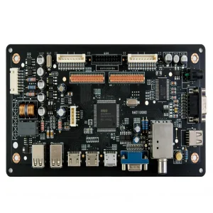
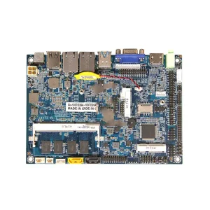
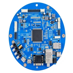
Submit your Gerber RS-274X files and Bill of Materials today. Our engineering department executes full DFM/DFA feasibility reviews and returns itemized pricing proposals backed by NDA within 24 hours.
