Discover our mission-critical printed circuit board assemblies engineered for automotive, industrial IoT, clean energy, and healthcare applications.

China Solar Street Light Controller PCB Assembly Manufacturers, Service
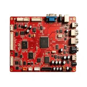
OEM Car Navigation Systems PCBA Assembly--STHL Manufacturer, Manufacturers
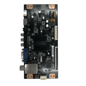
OEM LED Signage Board PCB Assembly--STHL Manufacturer, Factory
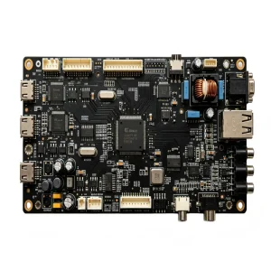
OEM Wireless Network Routers PCBA Assembly--STHL Manufacturers, Factory
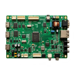
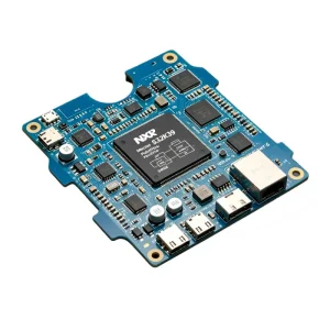
High-Quality Anesthesia Machine PCB Assembly--STHL Manufacturer, Manufacturers
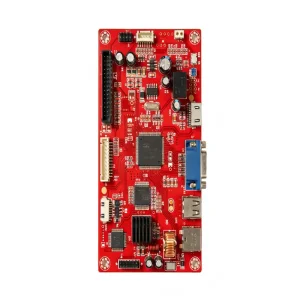
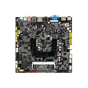
Navigating regional microelectronics specialization, raw material supply dynamics, and high-density semiconductor interconnect integration.
The contemporary printed circuit board (PCB) fabrication industry represents an indispensable foundation of the global digital economy, expanding beyond conventional substrate interconnects toward complex, multi-functional system-in-package platforms. Globally, the PCB market exceeds eighty billion dollars annually, propelled by relentless structural transitions in artificial intelligence compute nodes, high-voltage electric vehicle (EV) powertrains, medical telemetry, and satellite communications.
While design centers in North America and Western Europe drive silicon conceptualization and firmware innovation, over 75% of global high-density interconnect (HDI) and multilayer substrate fabrication remains concentrated in the Asia-Pacific region—predominantly within the Greater Bay Area of China. Shenzhen serves as the global epicenter for fast-turn prototyping and high-reliability volume fabrication. Shenzhen STHL Electronics Co., Ltd. (founded in 2006) leverages this geographic synergy, providing international OEMs with tier-one component procurement, copper foil trace integrity, and sub-surface microvia reliability without the friction of decentralized supply channels.
Recent macroeconomic disruptions have highlighted the strategic necessity of supply chain resilience. Global electronics manufacturers can no longer afford fractured manufacturing lifecycles where design, raw board lamination, active component kitting, and SMT assembly occur across disparate geographic silos. Fragmented hand-offs introduce uncontrolled thermal mismatches, solder mask oxidation, and intellectual property exposure. STHL eliminates these vulnerabilities by uniting precision board fabrication, global silicon sourcing, surface mount technology, automated optical inspection, and complete box-build integration under a single verified quality umbrella.
With sub-3nm semiconductor node packaging adopting 2.5D/3D chiplets, standard FR-4 gives way to ultra-thin cores, low-loss BT resins, and Substrate-Like PCBs (SLP) demanding micro-line resolutions under 25µm.
Automotive (IATF 16949) and life-support medical electronics (ISO 13485) enforce absolute trace accountability down to reel lot IDs, automated reflow thermal thermal logs, and individual serial laser etching.
Wide-bandgap semiconductors (SiC and GaN) demand heavy copper layers (up to 6oz+), ceramic cores (AlN/Al2O3), and direct copper bonding (DCB) to handle extreme thermal dissipation in compact footprint designs.
Combining 10,000+ m² of ISO-certified cleanroom manufacturing with 7 high-speed SMT lines, advanced DIP insertion, and automated functional testing.
Shenzhen STHL Electronics Co., Ltd. represents the premier echelon of high-mix, variable-volume PCB fabrication and electronic contract manufacturing. Operating from our Bao'an smart manufacturing facility in Shenzhen, we provide end-to-end realization for hardware designers, venture-backed startups, and Fortune 500 industrials across 90+ countries including Germany, the United States, Japan, and the UK.
Our infrastructure operates under rigorous digital governance. Utilizing centralized Enterprise Resource Planning (ERP) tightly unified with automated Manufacturing Execution Systems (MES), every single board assembly is tracked through every solder paste printing cycle, pick-and-place placement coordinate, 10-zone reflow thermal curve, and 3D X-ray inspection record. This level of deterministic manufacturing control guarantees zero component drift, eliminated cold-solder bridges, and full batch traceability.
Tailoring dielectric core selections, copper foil grain structures, and surface finishes to real-world industrial, medical, and aerospace operating environments.
Designed in accordance with IPC-6012DA Class 3 and IATF 16949. Incorporates 77GHz radar PTFE laminate transitions, blind/buried microvias, conformal acrylic coating, and high thermal cycle resistance (-40°C to +150°C).
Strict adherence to ISO 13485 standards. Assemblies for anesthesia control, surgical displays, and drug infusion mechanisms feature ENIG surface finishes, ionic contamination testing, and non-destructive 3D CT scanning.
High-reliability Primary Flight Displays (PFD) and aerospace navigation computers fabricated with polyimide core laminates, heavy copper heat planes, conformal parylene deposition, and vibration-proof THT anchoring.
Ruggedized controller boards for automated assembly robotics, variable frequency drives, and industrial firewall appliances featuring high-voltage isolation slots, optocoupler protections, and heavy copper power routing.
Smart solar controllers, microinverters, and high-efficiency BMS motherboards designed with aluminum metal-core PCBs (MCPCB), thick FR-4 multilayer stacks, and low ESR electrolytic capacitor stabilization.
High-speed Wi-Fi 7 wireless gateways and smart speakers integrating multi-layer impedance-controlled differential pairs (100Ω ±5%), staggered laser microvias, and low dielectric loss Rogers / Megtron 6 substrates.
From initial Gerber DFM audit to box-build integration and international cold-chain air logistics.
Comprehensive multi-layer Gerber, netlist, and centroid check. Our senior engineers verify drill aspect ratios, thermal reliefs, impedance targets, and solder bridge clearances prior to tooling release.
Full traceability sourcing through franchised master distributors (Digi-Key, Mouser, Arrow, Avnet) and verified original manufacturers. Full lot trace integrity with incoming counterfeit microscopy inspection.
Inner layer imaging, acid etch chemistry, direct laser imaging (LDI), high-pressure vacuum lamination, mechanical/CO2 laser microvia drilling, horizontal pulse copper electroplating, and LPI solder masking.
Automated solder paste jet printing with closed-loop 3D SPI. High-speed Yamaha and Panasonic placement heads mounting down to 01005 passives and 0.3mm pitch BGAs under nitrogen-atmosphere 10-zone reflow.
100% post-reflow 3D automated optical inspection verifying component presence, polarity, tombstoning, and solder meniscus volume. Transmission X-Ray microtomography verifying BGA void ratios under 10%.
Automated selective soldering and wave soldering for through-hole connectors. Automated robotic selective conformal coating (polyurethane, silicone, acrylic) to safeguard against harsh condensation and salt mist.
Bed-of-nails in-circuit testing, automated firmware flashing, custom test jig functional verification, custom anti-static hermetic vacuum packing, and priority air freight to worldwide destinations.
Verified manufacturing bounds for multilayer rigid, high-density interconnect (HDI), and flex-rigid electronics.
| Fabrication Parameter | Standard Capability | Advanced / Frontier Limits | Verification Protocol |
|---|---|---|---|
| Layer Count (Rigid) | 1 to 32 Layers | Up to 64 Layers (Backdrill Available) | Cross-Section Microsectioning |
| HDI Construction | 1+N+1, 2+N+2 Microvia | Any-Layer HDI (ELIC / mSAP) | Laser Micro-profilometry |
| Min. Line Width / Spacing | 3.0 mil / 3.0 mil (75µm) | 1.8 mil / 1.8 mil (45µm) | Automated Optical Inspection (AOI) |
| Substrate Base Materials | Standard FR-4, High-Tg (TG170/180) | Rogers, Nelco, Isola, Teflon, Aluminum Core, Ceramic | TGA / DSC Thermal Analysis |
| Minimum Microvia Diameter | 0.20 mm (Mechanical) | 0.075 mm / 3 mil (UV/CO2 Laser) | X-Ray Transmission Gauging |
| Finished Copper Thickness | 0.5 oz to 3.0 oz | Up to 12.0 oz (Heavy Power Bus) | Eddy Current Resistance Probe |
| Surface Finishing Options | Lead-Free HASL, ENIG, OSP | Immersion Silver/Tin, ENEPIG, Hard Gold Finger | XRF Coating Thickness Meter |
| SMT Component Placement | 0201 passives, 0.4mm BGA | 01005 chips, 0.3mm ultra-fine pitch BGA/CSP | 3D AOI & 3D AXI Micro-CT |
Anticipating the technological inflections defining high-speed compute, AI accelerators, and extreme-environment substrates.
Transitioning beyond organic resins toward glass-core interposers delivering near-zero warpage, superior mechanical stiffness, and embedded optical waveguides for co-packaged optics (CPO) architectures.
Deploying real-time neural network vision models on SMT pick-and-place nozzles to dynamically correct rotational offsets and solder volume variations before reflow, reducing rework cycles to zero.
Standardizing recyclable bio-based epoxies, water-soluble temporary masks, and ultra-low carbon electrolytic copper foils to comply with emerging EU circular economy mandates and global RoHS/REACH standards.
Direct answers to the most stringent engineering and supply chain inquiries submitted by global technical leads.
We purchase 100% directly from verified original manufacturers or their authorized tier-one global distributors (Digi-Key, Mouser, Arrow, Avnet, Element14). Incoming components undergo rigorous inward receiving verification, including barcode validation against factory manifests, high-magnification optical marking inspection, and acetone wash testing for re-marked parts.
We do not impose any Minimum Order Quantity. Our flexible lines support quick-turn engineering prototypes (from 1 to 10 boards) through low-volume initial production (NPI) to sustained high-volume series runs of millions of units, seamlessly transitioning across the exact same equipment recipes.
We utilize Polar Instruments Si9000 electromagnetic field solver software for precise stack-up modeling. Tolerances for single-ended (50Ω) and differential pairs (90Ω, 100Ω) are held within ±10% standard, and down to ±5% upon request, validated via Time Domain Reflectometry (TDR) coupons on each panel border.
Customer IP security is governed by legally binding Non-Disclosure Agreements (NDAs) executed prior to any file transmission. All CAD datasets, schematic files, BOMs, and hex firmware binaries are housed on isolated, encrypted internal networks with strict biometric and role-based permissions.
We employ off-axis 3D Automated X-ray Inspection (AXI) and high-resolution microtomography systems capable of sub-micron defect detection. We measure ball circularity, solder bridge bridging, and total void area percentage to adhere strictly below IPC Class 3 limits (<15% total void area, <9% single void area).
Bare board quick-turn prototypes can be fabricated in as little as 24 to 48 hours for 2 to 4 layers. Full turnkey assembly (bare board fabrication, rapid component kitting, and SMT placement) typically finishes in 5 to 7 business days, with standard volume delivery spanning 2 to 3 weeks.
Examine our specialized sub-assemblies built for healthcare video monitors, mission-critical avionics, fire safety, and surveillance hardware.
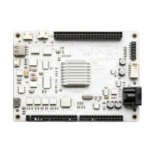
China Operating Room Video Monitoring System PCB Assembly--STHL Service, Factory
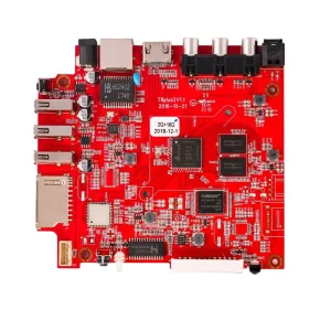
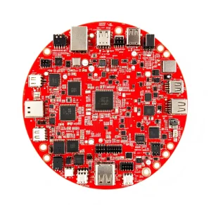

OEM Drug Delivery System PCB Assembly--STHL Manufacturers, Service
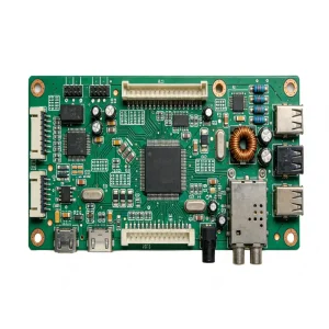
China Primary Flight Display (PFD) PCBA Assembly--STHL Manufacturer, Manufacturers
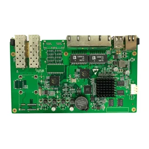
High-Quality Safety & Security PCBA Applications: Empowering Reliable Protection
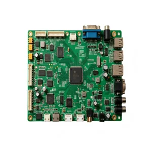
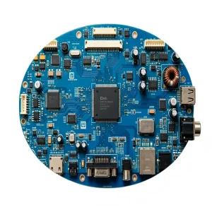
China Portable Wi-Fi Devices PCBA Assembly--STHL Manufacturer, Manufacturers
