From industrial server topologies and RF communication modules to life-critical medical imaging assemblies, explore our fully qualified electronic manufacturing production lines and rapid-scaling capabilities.
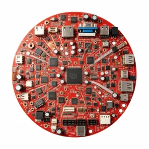
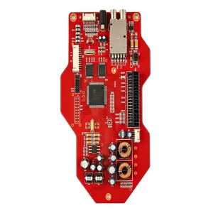
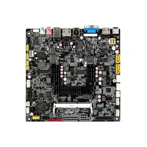

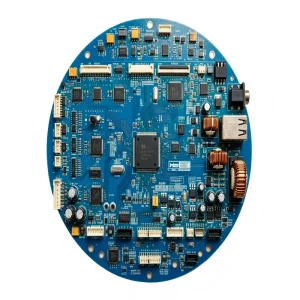
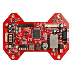
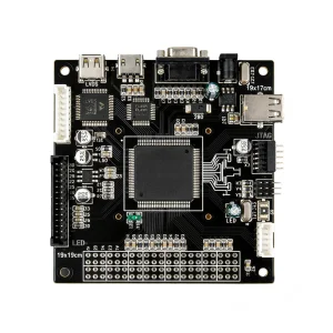
In the contemporary hardware engineering paradigm, high-quality PCB sourcing is no longer a simple transactional purchase of etched copper and soldermask. It has evolved into a strategic pillar of enterprise survival, operational continuity, and system-level performance. Electronics procurement directors, hardware engineering leads, and supply chain vice presidents operate within a volatile macroeconomic landscape defined by geopolitical disruptions, sudden component end-of-life (EOL) announcements, escalating semiconductor lead times, and rigorous international regulatory mandates.
Selecting an elite PCB manufacturing and assembly (PCBA) partner demands an analytical evaluation that bridges bare-board chemical metallurgy, surface-mount technology (SMT) automation thresholds, rigorous Bill of Materials (BOM) forensic validation, and total cost of ownership (TCO) predictability. A single substandard via barrel, an untraced counterfeit passive component, or an unmitigated solder void beneath an ultra-fine-pitch Ball Grid Array (BGA) can jeopardize an entire deployment, resulting in catastrophically expensive warranty recalls and reputational loss.
Core Procurement Paradigm: World-class Electronics Manufacturing Services (EMS) rely on single-source accountability. Fragmenting the manufacturing lifecycle between independent PCB fabrication plants, separate component brokers, and disconnected assembly houses introduces friction, finger-pointing during fault isolation, compounded logistics tariffs, and uncoordinated quality audits. STHL consolidates these disparate phases into a synchronized, single-roof production infrastructure operating under rigorous ISO 9001, IATF 16949, ISO 13485, and ISO 14001 governance.
Strategic purchasing demands structural de-risking across every tier of the manufacturing supply chain. We analyze the 4 foundational pillars required to secure sustained operational stability.
Component obsolescence occurs without warning. Our engineering teams perform deep parametric scrubbing of your Bill of Materials during preliminary RFQ review. By identifying single-source ICs, approaching Lifecycle End-of-Life (EOL), and engineering form-fit-function (FFF) second-source drop-in replacements, we shield programs from sudden factory shutdowns and unbudgeted redesign cycles.
With gray-market risks persisting worldwide, authentic component sourcing is non-negotiable. Operating with direct authorized distribution networks—including Arrow, Avnet, Digi-Key, Mouser, Farnell, and franchised tier-1 factory direct channels—STHL enforces incoming material verification protocols conforming to IDEA-STD-1010 and AS6081 aerospace inspection principles.
Quality begins inside the inner copper layers. We source certified copper clad laminates (CCL) directly from industry leaders such as Shengyi, Isola, ITEQ, and Rogers. Every fabricated panel features edge-routed matrix datamatrix tracking, linking glass weave styles, Tg/Td glass transition ratings, and copper foil adhesion metrics directly to the MES database.
Prototypes validated on separate cottage-industry hand lines frequently fail when transferred to high-speed automation. At STHL, New Product Introduction (NPI) prototypes run on the identical high-precision surface mount lines (Yamaha, Panasonic) that govern volume production, guaranteeing consistent thermal reflow profiling, stencil aperture geometry, and yield consistency.
Comprehensive manufacturing tolerances and material science standards executed across our Shenzhen production facilities, engineered to surpass IPC Class 2 and Class 3 aerospace/medical specifications.
| Engineering Parameter | Standard Capability | Advanced / HDI Precision Threshold | Inspection & Verification Standard |
|---|---|---|---|
| Layer Count & Stackup | 1 – 28 Layers (Rigid FR-4) | Up to 64 Layers; 1-4 Stage Any-Layer HDI, Rigid-Flex | X-Ray Layer Alignment & Microsection Metallography |
| Trace Width / Spacing (L/S) | 3.5 mil / 3.5 mil (90µm / 90µm) | 2.0 mil / 2.0 mil (50µm / 50µm) via mSAP Semi-Additive | Automated Optical Inspection (AOI) with AI Defect ID |
| Microvia / Laser Drill Geometry | 0.20 mm (8 mil) Mechanical | 0.075 mm (3 mil) UV / CO2 Laser Microvias; Via-in-Pad Plated (VIPPO) | Field Emission Scanning Electron Microscopy (FE-SEM) |
| Base Copper & Plating Aspect Ratio | 0.5 oz – 3 oz; 8:1 Aspect Ratio | Up to 12 oz Heavy Copper; 14:1 Through-Hole Plating Ratio | Eddy Current Measurement & Cross-Section Coulometry |
| SMT Placement & Component Size | 0201 passives, 0.4mm pitch QFP | 01005 (0402 metric), 0.3mm pitch Micro-BGA, PoP (Package on Package) | 3D Solder Paste Inspection (SPI) + 3D Automated AOI |
| Solder Joint Integrity & Voiding | IPC-A-610 Class 2 (<25% Voiding) | IPC-A-610 Class 3 (<10% Voiding on QFN/BGA thermal pads) | High-Resolution 3D Computed Tomography / Offline AXI |
| Surface Finishes & Metallurgy | HASL Lead-Free, OSP, ENIG (Electroless Nickel Immersion Gold) | ENEPIG, Immersion Silver/Tin, Hard Gold Plating (30µ"), Selective ENIG | X-Ray Fluorescence (XRF) Coating Thickness Analysis |
Design for Manufacturability (DFM) & Assembly (DFA) Integration: Prior to releasing any tooling film or fabricating laser stencils, our 50+ member engineering team executes automated Valor NPI / Genesis CAM design simulations. We identify high-risk anomalies such as acid traps, starved thermal reliefs, insufficient solder dam margins, shadowed THT pins during wave soldering, and unbalanced copper distributions that generate thermal bow and twist during lead-free SAC305 reflow profiles.
In high-rel applications, quality cannot be inspected into a product—it must be engineered into every thermodynamic, mechanical, and logistical process step.
Stringent compliance with Advanced Product Quality Planning (APQP), Production Part Approval Process (PPAP Level 3), Failure Mode and Effects Analysis (FMEA), and statistical process control (SPC). We enforce strict Cpk > 1.67 monitoring on critical paste printing and component centering variables.
Dedicated medical device PCBA protocols ensuring comprehensive risk management (ISO 14971), validated wash-free residue limits, strict bio-burden control, ionic contamination testing via ROSE testing (<1.56 µg/cm² NaCl equivalent), and total Device Master Record (DMR) archiving for 10+ years.
Every single manufactured circuit board is laser-engraved with an individual high-density 2D DataMatrix code. Our Manufacturing Execution System (MES) links every serial number to the specific solder paste batch, placement feeder slot, reflow thermal profile curve, AOI imagery, and functional test vector results.
Specific operational architectures tuned to the mechanical, environmental, and thermal stresses of demanding operating environments.
From Battery Management Systems (BMS) with high-voltage isolation barrier testing to ADAS LiDAR control units, we build to withstand severe thermal cycling (-40°C to +125°C), high mechanical vibration, and moisture ingress utilizing selective automated silicone/polyurethane conformal coatings.
Deploying server firewalls, high-throughput network switches, and optical transceiver line cards. We manage high-speed differential pairs exceeding 56 Gbps PAM4, backdrill stubs to suppress signal reflections, and enforce controlled dielectric tolerances within ±5% across megahertz and gigahertz spectrums.
Industrial PLC modules, ruggedized power distribution units, and safety leak detectors operating continuously in caustic atmospheric conditions. We implement heavy copper power buses (3oz to 6oz), optocoupler isolation clearances, creepage and clearance compliance per IEC 61010, and conformal potting.
Anticipating the next wave of edge AI computing, micro-miniaturization, and thermal dissipation challenges with continuous capital expenditure investment.
Integration of thin-film embedded resistors and decoupling capacitors directly inside CCL prepregs, reclaiming up to 40% surface SMT real estate for ultra-dense IoT and wearable medical micro-sensors.
Mass industrialization of 0.25mm ball-pitch stacking architectures, high-precision vacuum vapor phase reflow soldering to achieve <5% solder void thresholds across high-power automotive heterogenous computing modules.
Transition from pure copper differential transmission to embedded polymer optical waveguides within PCB layers, eliminating electromagnetic interference (EMI) bottlenecks in hyperscale 800G/1.6T networking topologies.
Pioneering ultra-low loss hydrocarbon and bio-composite resin matrices exceeding global RoHS 3 and REACH regulations, eliminating persistent polyfluoroalkyl chemicals while maintaining Dk < 3.0 and Df < 0.002 up to 110 GHz.
Detailed technical responses addressing the operational criteria sourcing managers and hardware engineering leads scrutinize prior to awarding enterprise manufacturing contracts.
Explore our advanced manufacturing execution across high-voltage BMS systems, satellite navigation transceivers, diagnostic medical radiography, and gigabit network interfaces.
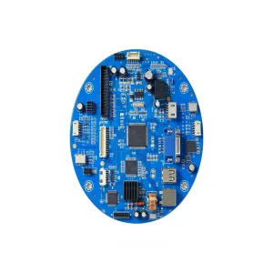
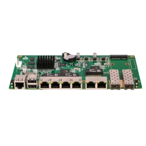
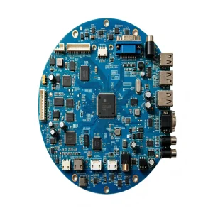

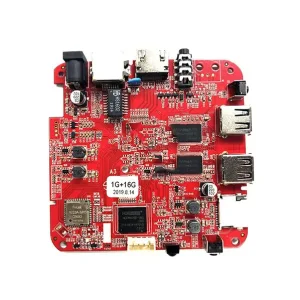
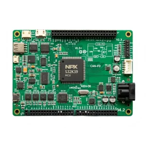
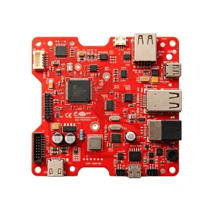
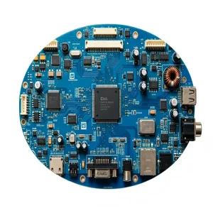
A transparent three-step pathway designed for purchasing committees, technical sourcing managers, and VP-level engineering leadership looking to initiate factory audits and RFQ evaluations.
We initiate the engagement through an enforceable mutual Non-Disclosure Agreement. Your engineering team submits the preliminary manufacturing file set: RS-274X or ODB++ Gerber files, consolidated Bill of Materials with manufacturer part numbers, pick-and-place XY centroid coordinates, and IPC acceptance class specifications.
Within 24 to 48 hours, STHL's senior CAM and manufacturing engineering leads return an exhaustive DFM/DFA diagnostic audit. This includes copper trace optimization, thermal relief sizing, solder dam clearances, BOM obsolescence alerts, cost-reduction recommendations, and an unbundled turnkey price quotation.
Upon sign-off, a pilot production batch (5 to 50 units) is scheduled. This run generates a complete First Article Inspection (FAI) report, microsection metallography records, X-Ray BGA void analysis, and thermal profile logs. Once approved, the project transitions smoothly to full-rate production without retooling overhead.
