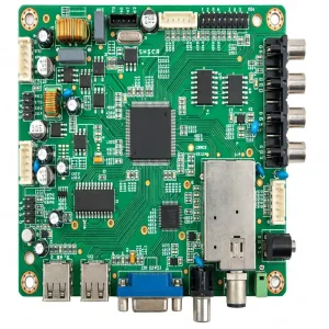
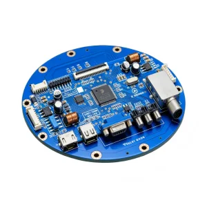
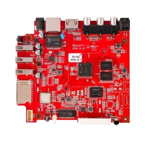
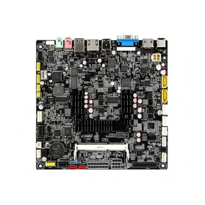
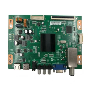
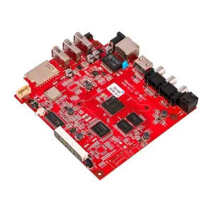
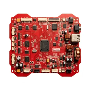
Discover our field-proven assemblies built for renewable energy, intelligent automotive units, satellite tracking, and IoT infrastructure.

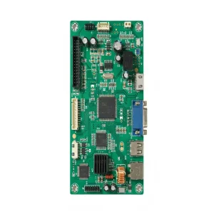
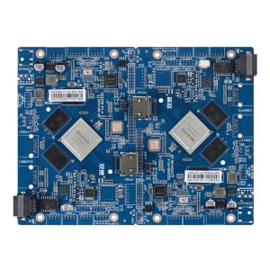
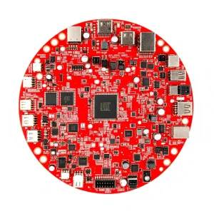

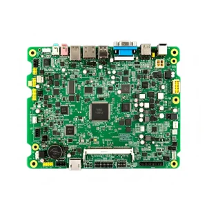
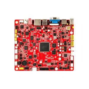
While often conflated in loose commercial jargon, the distinction between a Printed Circuit Board (PCB) and a Printed Circuit Board Assembly (PCBA) is foundational to supply chain risk mitigation, lifecycle costing, and failure mode analysis.
| Evaluation Parameter | Printed Circuit Board (PCB) | Printed Circuit Board Assembly (PCBA) |
|---|---|---|
| Definition & Nature | Passive unpopulated mechanical substrate featuring etched copper traces, vias, and pad layouts. | Fully functioning electronic assembly integrated with active, passive, and electro-mechanical parts. |
| Core Manufacturing Discipline | Subtractive/additive chemical processing, photolithography, laminating, drilling, copper plating. | High-speed SMT surface mounting, THT selective soldering, reflow profile tuning, automated testing. |
| Component & Supply Chain Scope | Copper clad laminates (FR4, Rogers, Polyimide), dry film, soldermask, noble metal platings (ENIG/Imm-Ag). | Semiconductors (MCUs, BGA, QFN), passives, passivated connectors, custom firmwares, cable harnesses. |
| Primary Verification Gate | Bare board flying probe testing, automated optical inspection (AOI), impedance TDR verification. | 3D SPI, automated X-ray inspection (AXI), in-circuit test (ICT), and functional operational validation (FCT). |
| Risk & Yield Accountability | Delamination, pad lifting, dielectric breakdown, dimensional distortion. | Solder bridges, tombstoning, cold joints, component obsolescence, ESD events, functional firmware faults. |
Traditional procurement decouples bare board fabrication from assembly houses, introducing latency, logistical compounding, and ambiguous failure accountability. Turnkey EMS systems reconcile this fracture.
Eliminate production delays before capital expenditure. Senior engineering reviews assess thermal relief layouts, tombstoning risks, pad geometry discrepancies, and high-speed signal integrity to avoid re-spins.
Sourcing from vetted franchised distributors (Arrow, Avnet, Digi-Key, Mouser) guarantees counterfeit mitigation. Full lot-level trace identification ties individual board serials to factory production lots.
Eliminate commercial finger-pointing between bare board fabricators and SMT vendors. When quality escapes occur, a unified factory partner immediately diagnoses solder alloy metallurgy or delamination root causes.
Modern hardware brands operate in an era of heightened component volatility, geopolitical shifts, and compressed product release cycles. Sourcing leaders must balance cost with supply agility.
With critical semiconductor lead times fluctuating from 8 to 52 weeks, agile factories actively propose drop-in pin-compatible alternates and re-engineer PCB landing patterns on the fly.
Operating from Bao'an, Shenzhen gives STHL direct access to the world's most concentrated microelectronics supply cluster, reducing component lead times from weeks to hours.
Eliminate production bottlenecks by validating small engineering pilot runs (10-50 units) on identical multi-zone reflow SMT lines used later for 500,000-unit continuous mass manufacturing.
Quality assurance requires rigorous, third-party audited adherence to global standards across automotive, healthcare, and telecommunication sectors.
Stringent defect prevention, APQP workflows, and PPAP readiness designed for demanding vehicle electrification systems and powertrain control.
Standardized risk management and complete component traceability protocols for mission-critical life-support, diagnostic, and telemetry hardware.
Controlled continuous quality management and ecologically responsible production aligned with RoHS, REACH, and IPC-A-610 Class 2/3 criteria.
Enforceable bilateral NDAs precede all Gerber, schematic, and firmware transmissions, with encrypted air-gapped data access for all customer designs.
Our turnkey assemblies operate in mission-critical environments around the globe, from subsea telemetry systems to smart urban micro-grids.
Heavy-copper substrates and high-voltage isolation architectures for wind power controllers, solar microinverters, and high-efficiency battery management systems (BMS).
Designed to withstand harsh temperature cycling (-40°C to +125°C), continuous vibration, and thermal shock inside modern electric and autonomous vehicle platforms.
Multi-layer Rogers and high-Tg hybrid laminates engineered with controlled dielectric constants to minimize signal attenuation in optical network units (ONU) and 5G cellular arrays.
As components shrink toward 01005 footprints and thermal loads surge, our facility continually advances its hardware and process capabilities.
Integrating 0.3mm ultra-fine pitch Ball Grid Arrays, 01005 micro-passives, and Package-on-Package (PoP) assemblies with nitrogen reflow chambers to minimize oxidation.
Heavy-copper boards (up to 6 oz), embedded aluminum backing, and ceramic substrates designed to dissipate heat from wide-bandgap GaN and SiC power semiconductors.
Automated 3D AOI and real-time volumetric X-ray (AXI) platforms powered by machine vision algorithms identify solder voiding and micro-bridging below 10% tolerance thresholds.
Clear, detailed answers addressing common challenges in bare board procurement, assembly processes, quality assurance, and lifecycle management.
Browse our specialized assemblies engineered for heavy equipment, avionics, enterprise networking, and robotics.