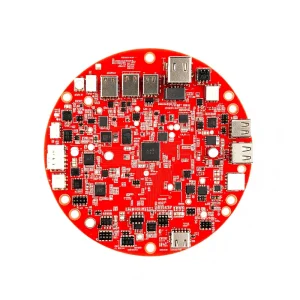
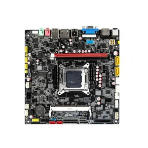
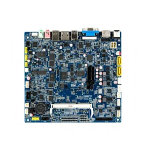
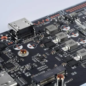
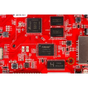
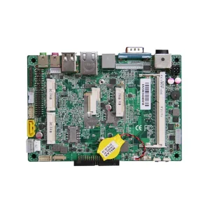
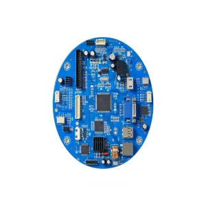
Production-ready sub-systems manufactured under zero-defect IPC-A-610 Class 3 specifications.
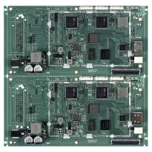

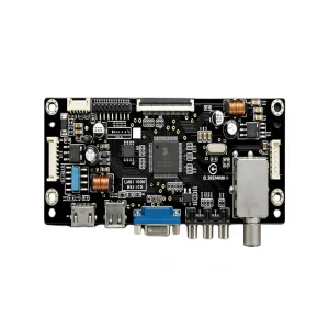
Analyzing the tectonic shifts toward high-mix low-to-mid volume manufacturing, miniaturization, and supply-chain resilience.
In modern industrial systems, the Printed Circuit Board Assembly (PCBA) is no longer merely an interconnect between discrete passive elements and integrated silicon. It represents the foundational nervous system of Industry 4.0 automation, next-generation medical therapeutics, advanced automotive autonomy, and smart grid orchestration. As global markets transition toward edge computing and high-density packaging, the parameters that define a viable manufacturing partner have evolved drastically.
Today's electronics Original Equipment Manufacturers (OEMs) operate in an environment conditioned by relentless component volatility, shrinking silicon footprints (such as 01005 passives and 0.3mm pitch Ultra-Fine BGAs), and tighter compliance mandates under IATF 16949, ISO 13485, and ISO 9001. Contract manufacturing can no longer function purely as a downstream assembly line; it requires deep DFM (Design for Manufacturability), DFA (Design for Assembly), and DFT (Design for Testing) integration straight from the initial gerber prototyping stage.
While discussions regarding regional re-shoring dominate Western boardrooms, the global electronics industry remains deeply rooted in mature cluster ecosystems. The geographic concentration of raw laminates, passive component warehouses, precision metal fabrication, and packaging tooling within the Pearl River Delta enables turnaround speeds that cannot be matched in decentralized markets.
Mission-critical applications demand strict adherence to IPC Class 3 criteria. Whether managing voiding control under QFN thermal pads through 3D automated X-ray inspection (AXI) or preventing dendrite growth with precision selective soldering and conformal coating, reliability stems from verified automated closed-loop feedback systems.
Data integrity governs high-level electronics manufacturing. Modern contract manufacturing enforces total serialization: 2D matrix laser marking tracks bare boards, reel lot numbers, reflow thermal profiles, AOI images, and functional test logs directly to an institutional ERP/MES cloud infrastructure.
Why Tier-1 global developers leverage Shenzhen’s industrial density for strategic agility.
Shenzhen's 1-hour sourcing radius allows engineering changes (ECNs) and component swap-outs to happen in hours rather than weeks. Prototyping seamlessly shifts into pilot runs and volume SMT without cross-vendor delays or redundant tooling recharges.
STHL maintains an engineering team with over two decades of PCB fabrication, SMT surface-mount technology, and firmware flashing expertise. Every project undergoes full DFM screening to eliminate tombstoning, bridge risks, and cold solder anomalies prior to machine loading.
From multi-layer bare boards (HDI, Flex, Rigid-Flex) to turnkey components sourcing via Arrow, Avnet, DigiKey, and verified franchise agents, through to custom wire harness assembly, potting, ultrasonic welding, and final retail box packaging ready for distribution.
Addressing the top criteria international supply chain heads and procurement directors evaluate.
Procurement teams demand active lifecycle tracking. Our engineering team flags end-of-life (EOL) and not-recommended-for-new-designs (NRND) parts during quotation, offering drop-in footprint-compatible alternatives to avert sudden redesign halts.
Confidentiality is an absolute baseline. Hardware architecture, proprietary Gerber files, CAD layouts, firmware hex code, and proprietary manufacturing procedures remain protected under binding legal NDAs with segmented server isolation.
Wearables, aerospace modules, and medical probes require microvias, laser drilling, and staggered structures. SMT factories must hold sub-micron placement tolerance down to ±0.03mm, backed by real-time SPI (Solder Paste Inspection) optical feedback.
| Certification | Audit Scope & Industrial Relevance | Quality Assurance Protocols | Customer Beneficiaries |
|---|---|---|---|
| IATF 16949 | Automotive electronic systems, powertrain, ADAS, BMS | PPAP Level 3, FMEA, CP, SPC statistical control | Automotive Tier-1 & EV Manufacturers |
| ISO 13485 | Medical diagnostic boards, implantable devices, monitoring | Batch traceability, cleanroom assembly, bio-burden audits | Medical Equipment OEMs & Clinicians |
| ISO 9001 | General quality management, documentation, process loops | Internal corrective actions (CAPA), 8D troubleshooting | Industrial Automation & Smart Energy |
| ISO 14001 | Environmental management, chemical storage, RoHS & REACH | Lead-free soldering processes, hazardous waste filtration | Global Eco-certified Consumer Electronics |
Engineered to perform in severe operational environments with extreme vibration, moisture, and heat.
PLC controllers, motor inverters, and machine vision motherboards built with heavy copper (up to 6oz), high-Tg substrates, and automated conformal coating to endure chemical vapors, heat cycling, and electromagnetic interference.
Solar module monitors, micro-inverters, and power metering PCBA assemblies equipped with advanced thermal management, high-voltage creepage insulation, and rigorous surge testing to guarantee 10-25 years field endurance.
Precision drug delivery infusion systems, particle monitors, and patient wearable monitors manufactured in ESD Class 0 environments, utilizing 100% AOI, functional bed-of-nails verification, and complete serial lot traceability.
Transparent technical and commercial insights for engineering heads, supply chain managers, and hardware founders.
Quick-turn prototype runs can be completed within 24 to 48 hours following component procurement and engineering DFM approval. Mass production standard lead times typically range from 15 to 25 working days, heavily governed by specific long-lead active semiconductor components.
We source directly from original semiconductor manufacturers or verified global franchise distributors (Arrow, Avnet, DigiKey, Mouser). Incoming inventory is inspected at our incoming inspection facility via X-ray packaging inspection, marking verification, and solderability testing.
No. STHL operates with zero MOQ restrictions. We partner with clients from single-board engineering proof-of-concept (POC) prototypes, scaling into low-volume high-mix (HMLV) batches, through to continuous recurring mass-production runs on identical high-speed Yamaha and Fuji SMT lines.
Our quality regime encompasses 3D SPI (Solder Paste Inspection), 3D automated optical inspection (AOI), high-definition 2D/3D X-ray inspection for BGA/QFN void verification, In-Circuit Testing (ICT), Functional Circuit Testing (FCT), burn-in aging chamber stress tests, and automated conformal coating thickness measurement.
Yes. Our engineering procurement team continuously analyzes BOM health. When obsolete components or excessive lead-time parts are detected, we formulate a engineering proposal recommending drop-in pin-to-pin compatible alternatives or circuit adjustments with verified simulation models.
To provide a formal DFM review and quotation within 24 hours, we require: (1) Gerber files (RS-274X or ODB++), (2) Complete Bill of Materials (BOM) with manufacturer part numbers and reference designators, (3) Pick and Place / Centroid coordinates (XY file), and (4) Functional testing instructions if FCT is required.
Scalable electronic manufacturing solutions across telecommunications, power, and environmental sensors.