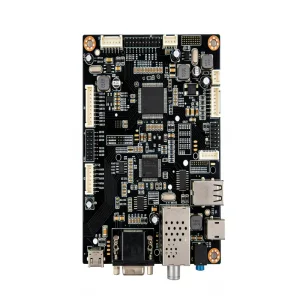
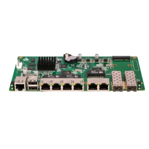
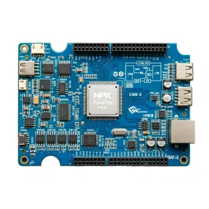
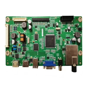
Rapid prototyping and turnkey box build solutions across renewable power, automotive systems, IoT telemetry, and high-frequency DC conversion.
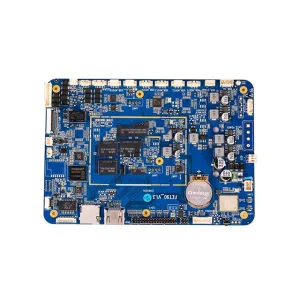
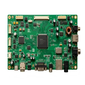
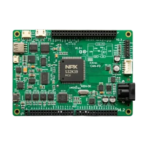
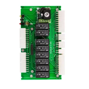
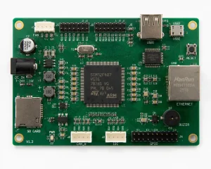

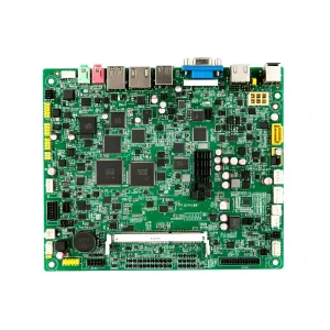
Prototyping in modern electronics engineering is no longer simply about soldering components onto copper clad. It is a rigorous, iterative discipline governed by IPC-A-610 Class 2/3 criteria, controlled impedance tolerance (±5%), advanced thermomechanical profiling, and strict Design for Excellence (DFX) guidelines.
Every prototype layout undergoes thorough Gerber and netlist scrutiny. We eliminate thermal sink imbalances, avoid solder bridge hazards in fine-pitch 0.3mm BGA packages, verify tombstone risks on 01005 passives, and align fiducial markers for sub-micron robotic pick-and-place accuracy.
Rapid pilot fabrication covers standard FR-4 (Tg 150-180°C), flex and rigid-flex laminates, high-frequency Rogers/PTFE substrates, heavy-copper industrial power boards, and high-density interconnect (HDI) configurations featuring laser-drilled microvias (1+N+1 to any-layer HDI).
Supporting hardware innovators through Engineering Verification Testing (EVT), Design Verification Testing (DVT), and Production Verification Testing (PVT). Our flexible SMT lines run seamless low-to-medium lot conversions without recurring engineering bottlenecks.
The Greater Bay Area—specifically the Bao'an electronics cluster in Shenzhen—represents the densest electronics component and PCB manufacturing ecosystem in the world. Operating within this epicenter gives STHL unprecedented lead-time compression and agile responsiveness that overseas facilities simply cannot replicate.
Our direct vendor relationships with over 100 franchised semiconductor distributors—including Arrow, Avnet, Digi-Key, Mouser, and STMicroelectronics—provide verified access to over 500,000 active part numbers. By pairing localized supplier links with in-house real-time ERP pricing engines, we mitigate lifecycle risks, combat part obsolescence with viable pin-compatible alternate suggestions, and enforce rigorous anti-counterfeit protocols.
Incoming raw electronic materials pass through mechanical dimension checks, solderability assessments, decapsulation inspection, and internal X-ray imaging before staging in moisture-barrier, ESD-regulated storage cabinets.
As computational density accelerates and electronic devices become increasingly miniaturized, prototype PCBA production is adopting cutting-edge automated assembly paradigms. We continuously upgrade our line capabilities to match advancing semiconductor packaging architectures.
Deploying fine-pitch wire bonding, flip-chip, and System-in-Package (SiP) modules directly alongside micro-BGA components for edge AI microcontrollers and ultra-compact wearable devices.
Utilizing real-time deep neural networks to automate defect detection in solder paste volume (3D SPI), hidden solder voiding under QFN/BGA packages via high-resolution 3D X-ray inspection.
Full compliance with RoHS 3 and REACH regulations. Nitrogen-purged 10-zone reflow profiles reduce intermetallic compound oxidation while sustaining void levels below 10% on power MOSFETs.
End-to-end industrial IoT integration connecting solder paste printers, pick-and-place feeders, reflow ovens, and test jigs to a unified Manufacturing Execution System (MES) for trace-level accountability.
Every industry presents unique mechanical, electrical, and regulatory requirements. Our engineering team customizes the assembly stack-up, solder alloys, conformal coatings, and test routines to match exact operating conditions.
| Industrial Sector | Key PCBA Engineering Challenges | Standards & Quality Mandates | STHL Quality Safeguards |
|---|---|---|---|
| Automotive Electronics | Extreme temperature cycling (-40°C to +125°C), vibration endurance, high current loads. | IATF 16949, AEC-Q100/200, IPC Class 3 | AOI/AXI 100% inspection, potting, conformal coating, automated high-pot dielectric testing. |
| Medical & Healthcare | Zero-defect tolerance, patient isolation, sensor signal purity, bio-compatible cleanliness. | ISO 13485, FDA GMP, IPC Class 3 | Cleanroom assembly zones, serialized component lot traceability, rigorous FCT bench verification. |
| Industrial Control & Energy | Continuous 24/7 duty cycles, high-voltage isolation, corrosive atmospheric environments. | ISO 9001, UL 94V-0, CE, RoHS | Thick copper traces, robotic selective conformal coating, thermal shock chamber validation. |
| Telecom & Edge Computing | High-frequency RF signal integrity, fine-pitch multi-gigahertz processors, dense routing. | IPC-6012, IEEE Standards, FCC | Controlled impedance routing (±5%), low-loss substrate handling, 0.3mm BGA placement precision. |
Intellectual property protection is the cornerstone of our global partnerships. We sign legally binding Non-Disclosure Agreements (NDAs) prior to file intake. Gerber files, schematics, and proprietary firmware are stored in compartmentalized encrypted servers accessible solely by authorized project personnel.
We ensure that assemblies satisfy the regulatory requirements of all destination markets. From European CE, RoHS, and REACH directives to North American FCC and UL testing, our manufacturing lines ensure full material documentation, certificates of conformance (CoC), and conflict-free mineral declarations.
Eliminate misunderstandings with our dedicated team of bilingual electrical and mechanical engineers. We communicate via technical engineering queries (EQs), real-time video conferencing, and detailed DFM feedback reports, bridging time zones to keep your project moving without delays.
Every project at STHL follows an audited, repeatable workflow with milestone gates to guarantee that physical hardware perfectly mirrors your CAD intent.
Comprehensive verification of Gerber files, Bill of Materials (BOM), pick-and-place centroid coordinates, and thermal profile simulations.
Sourcing components via authorized global distributor channels. Lot code verification, moisture sensitivity level (MSL) checks, and anti-counterfeit testing.
Automated solder paste printing, 3D SPI volume inspection, Yamaha/Panasonic high-speed component placement, and multi-zone reflow soldering.
Optical 3D AOI, high-definition X-ray (AXI), flying probe testing, in-circuit testing (ICT), and full custom functional verification testing (FCT).
Essential technical and procurement insights for hardware engineers, project managers, and sourcing professionals.
From precision medical imaging to automotive ADAS edge processors and high-bay solid-state lighting—engineered with zero-defect quality control.