
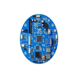
Proven engineering architectures manufactured in our Class 100,000 dust-free facility, meeting the rigorous standards of aerospace, medical workstation instrumentation, and automotive mobility ecosystems.
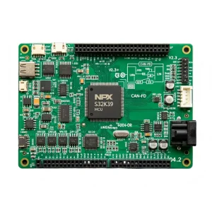

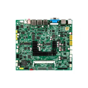
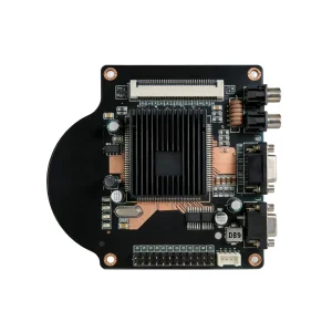
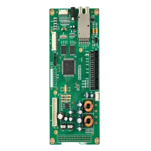

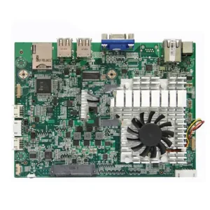
Shenzhen STHL Electronics Co., Ltd. delivers full-lifecycle Electronics Manufacturing Services (EMS). From high-complexity bare PCB fabrication and high-speed SMT assembly to full product integration (Box Build), we mitigate manufacturing risk for Tier-1 OEMs and ambitious hardware disruptors worldwide.
Every Gerber dataset, stack-up specification, and Pick-and-Place profile undergoes rigorous pre-production scrutiny. Our 50+ staff engineers optimize pad clearances, aspect ratios, and thermal relief configurations, preventing yield deficits before stencils are cut.
Deploying advanced SMT lines capable of handling 01005 passives, 0.3mm fine-pitch BGAs, CSPs, and micro-QFN packages with closed-loop optical feedback. 7 specialized SMT lines and 2 dedicated DIP lines offer seamless prototype-to-volume transition.
Quality gates anchored by 3D Automated Optical Inspection (AOI), 3D Solder Paste Inspection (SPI), high-resolution X-ray transmission radiography, Flying Probe, In-Circuit Testing (ICT), and full custom Functional Testing (FCT) jigs.
International technology leaders face rising supply-chain volatility, component obsolescence, and margin compression. STHL neutralizes these operational threats through centralized, turnkey manufacturing.
Mitigate gray-market and counterfeit threats. We secure silicon directly through franchised partners (Arrow, Avnet, Digi-Key, Mouser) backed by lot-level certificates of conformance.
Our component engineers suggest pin-compatible, drop-in equivalent active and passive parts for high-priced or end-of-life (EOL) items, slashing BoM cost by up to 28% without redesigns.
Accelerate your NPI (New Product Introduction) cycles. We run 5-unit engineering pilot runs with the exact same industrial SMT tooling and profiles used for million-unit production.
From PCBA to shelf-ready electronics: potting, ultrasonic plastic welding, conformal coating, wire harnesses, custom packaging, labeling, and direct-to-warehouse fulfillment.
As electronics transition toward higher power densities, high-speed signals, and harsh environments, STHL continues to evolve its manufacturing tolerances, cleanroom standards, and inspection algorithms.
| SMT & Assembly Precision | Placement accuracy down to ±0.03mm (3 sigma); support for passive chips down to 01005 (0402 metric) and fine-pitch components down to 0.3mm pitch BGAs/CSPs. |
|---|---|
| Substrate Technologies | High-Tg FR-4, Aluminum Base (MCPCB), Rogers RF High-Frequency laminates, Polyimide Flex (FPC), Rigid-Flex combinations, Ceramic substrates, and Copper core thermal circuits up to 32 layers. |
| Thermal Profiling & Soldering | 10-temperature zone reflow ovens with closed-loop Nitrogen (N2) atmosphere control, selective wave soldering, and temperature-controlled robotic soldering stations. |
| Automated Quality Verification | In-line 3D SPI (Solder Paste Inspection), dual-camera 3D AOI (pre & post reflow), 100kV High-Resolution X-Ray with BGA voiding auto-calculation under 10%, Flying Probe test, and custom FCT load testing. |
| Environmental & Life-Cycle Protections | Automated selective conformal coating (polyurethane, acrylic, silicone), potting, clean-room wire harness assembly, firmware flashing, and burn-in temperature stress chambers. |
| MES & Industry 4.0 Traceability | Barcoded and laser-etched 2D DataMatrix board-level traceability linking individual component lots, reel IDs, SMT machine telemetry, and reflow thermal curves directly into ERP systems. |
International projects require flawless regulatory compliance. STHL's manufacturing infrastructure operates under stringent international certifications, backed by experienced logistics channels to over 90 destination markets.
Defect prevention, variation control, and APQP/PPAP documentation workflows tailored specifically for Tier-1 automotive sub-assemblies, EV motor drives, and telematics modules.
Risk mitigation strategies conforming to Class I, II, and III medical requirements. Controlled batch hygiene, electrostatic mitigation, and complete risk management documentation.
Seamless door-to-door delivery with cleared duties across North America (USA, Canada), Europe (Germany, UK, Italy, Poland), Latin America (Brazil, Argentina), and Asia-Pacific.
Explore our demonstrated capabilities across motion sensing, high-voltage power supplies, industrial telemetry, and optical transmission systems.
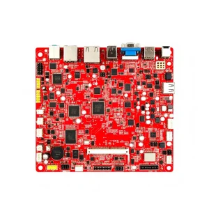
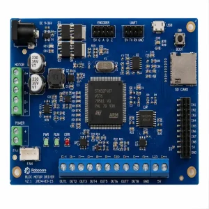

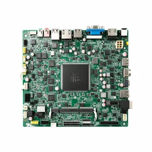
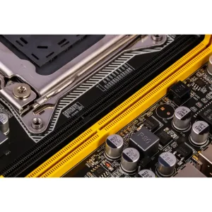
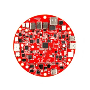
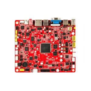
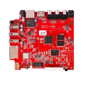
Achieving a 99% first-pass qualified shipment rate requires strict adherence to thermo-mechanical discipline, scientific solder profile modeling, and automated visual analytics.
Using laser-cut electro-polished stencils with nano-coatings alongside automated solder paste printers with real-time squeegee pressure feedback. 3D SPI measures paste volume down to micron tolerances to eliminate tombstoning and bridging.
Thermal sensors mapped directly to complex BGA joints guarantee that peak temperatures surpass the SAC305 liquidus point (217°C) without exceeding delicate IC junction thresholds (max 245°C), preventing internal micro-cracks and delamination.
For assemblies exposed to marine, automotive, or industrial chemical environments, our automated selective spray systems deposit uniform thin-film coatings with zero overspray, verified under UV blacklight inspection lamps.
Direct technical and commercial answers to simplify supplier onboarding, IP security audits, and multi-line production contracts.
To provide a definitive quotation and DFM assessment, we require: (1) Gerber RS-274X or ODB++ fabrication data; (2) Detailed Bill of Materials (BOM) detailing Manufacturer Part Numbers (MPN), approved alternate manufacturers, reference designators, and package footprints; (3) Pick-and-Place (XY Centroid) coordinate file; and (4) Functional Testing specifications and firmware instructions.
We maintain a rigorous vendor onboarding protocol. 100% of our electronic components are procured either factory-direct or via ISO-compliant franchised distributors (such as Arrow, Avnet, Digi-Key, Mouser, Future Electronics). Incoming parts undergo optical magnification, marking verification, pin oxidation analysis, and sample decapsulation testing where required.
Yes. STHL operates three flexible models: Full Turnkey (we procure bare boards, all passive and active parts, execute assembly, and final test), Partial Turnkey (client consign critical microcontrollers or specialized proprietary ASICs while we source commodity components), and Pure Consignment (client furnishes the complete BOM kit).
We execute standard bilateral Non-Disclosure Agreements (NDAs) prior to receiving proprietary Gerber datasets or firmware source files. Internally, design data is compartmentalized on isolated, access-restricted network servers with role-based authentication to safeguard customer IP.
For urgent NPI builds where components are locally in stock, our rapid SMT turnaround ranges from 24 to 72 hours following DFM resolution and bare PCB delivery. Standard turnkey production runs typically deliver within 15 to 20 working days, depending on component lead-times.
Our component engineers constantly monitor lifecycle trends through SiliconExpert and distributor APIs. If a component is marked for Last-Time-Buy (LTB) or Not Recommended for New Designs (NRND), we immediately alert your engineering department and propose drop-in pin-compatible alternatives to preserve uninterrupted assembly.