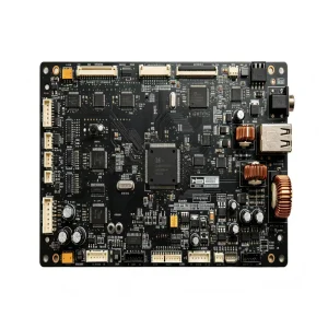
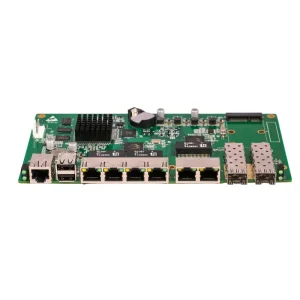
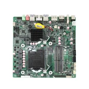
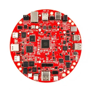
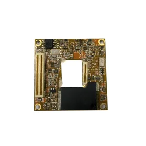
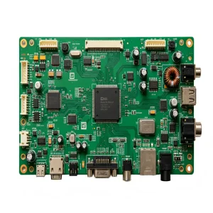
Explore production-grade assemblies manufactured with certified surface-mount placement precision, comprehensive DFM rules, and strict IPC-A-610 Class 3 workmanship criteria.
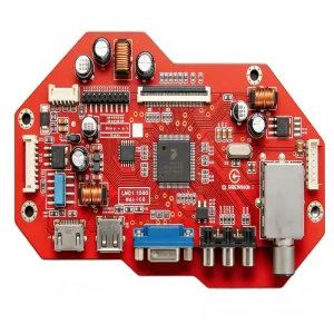
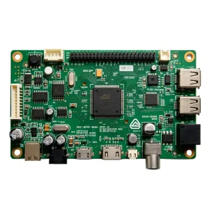
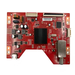
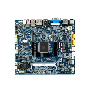

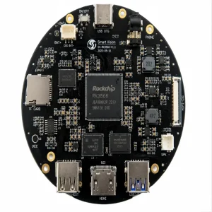
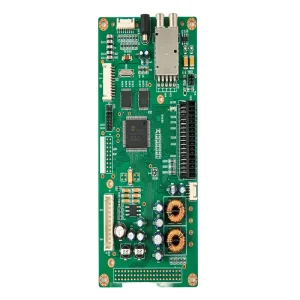
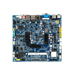
In modern electronic manufacturing services (EMS), Surface Mount Technology (SMT) capability represents far more than automated pick-and-place speed. It embodies micro-mechanical accuracy, closed-loop rheological paste measurement, advanced nitrogen thermal profiling, and comprehensive defect-suppression systems.
| SMT Technical Dimension | Current Production Baseline (STHL Standard) | Advanced / Next-Gen Capability | Verification & Quality Control Gateway |
|---|---|---|---|
| Passive Component Footprint | 0201 (0.6mm × 0.3mm), 0402, 0603, 1206 | 01005 (0.4mm × 0.2mm) & 03015 metrics | Closed-loop 3D Solder Paste Inspection (SPI) |
| IC & Array Packaging Pitch | QFP / QFN down to 0.4mm, BGA pitch ≥ 0.5mm | Ultra-fine BGA ≥ 0.3mm, CSP, PoP (Package-on-Package) | High-Magnification 3D AXI (Automated X-ray Inspection) |
| Placement Accuracy & Repeatability | ± 0.035mm (±35 μm) @ 3 Sigma | ± 0.020mm (±20 μm) with dynamic dual-vision fiducials | Optical linear encoder continuous calibration |
| Reflow Convection & Void Control | 10-zone hot-air convection with N2 atmospheric purge | Vacuum Reflow Chambers (≤ 5% total solder voiding) | Cross-section metallurgical microscopy & 3D CT scan |
| Substrate Dimension & Types | Max 510mm × 460mm; Rigid FR4, Metal Core, High-Tg | Rigid-Flex, Rogers RF, Ceramic, HDI Any-Layer | MES-coupled laser barcode tracking on board rail |
| Flux Chemistry & Cleaning | Lead-Free (SAC305, SAC0307), Halide-Free No-Clean | Water-Soluble chemistry with ultrasonic deionized wash | Ion chromatography cleanliness testing (<1.56 μg/cm² NaCl eq) |
The electronics manufacturing ecosystem is navigating a tectonic shift. As edge computing, automotive electrification, and mission-critical IoT demand unprecedented component density, international original equipment manufacturers (OEMs) face escalating complexity in selecting their EMS partners.
Micro-LED matrices, compact medical endoscopy boards, and optical transceivers demand component clearances down to 100 μm. Standard contract manufacturing lines fail where micro-bridging and tombstoning occur without adaptive solder paste stencil tensioning and closed-loop SPI-to-printer feedback.
While regional assembly hubs in the US and Europe serve strategic low-mix needs, the core volume of active semiconductor assembly, rapid tooling, and dense PCBA continues to rely on integrated industrial super-clusters. Leading companies leverage hybrid architectures: centralized SMT fabrication in specialized hubs coupled with agile regional distribution.
Industrial load balancers, energy controllers, and aerospace telemetry operate under cyclic temperature variations from -40°C to +125°C. High-quality SMT capability manufacturers eliminate joint fatigue through custom intermetallic compound (IMC) thickness control during nitrogen reflow.
Operating from Shenzhen STHL Electronics Co., Ltd.'s 10,000+ m² production complex in Bao'an District, our SMT ecosystem delivers unparalleled velocity. Shenzhen is the recognized heartbeat of global hardware innovation, offering an unmatched geographic concentration of fabrication, passive component distribution, and precision tooling.
Leveraging immediate proximity to primary component distributors and domestic silicon wafer fabrication, engineering changes (ECO) and prototype BOM releases transition from Gerber validation to live surface mount placement in as little as 48 hours without shipping lag.
STHL maintains active, audited sourcing pipelines with 100+ authorized global agents (including Arrow, Avnet, Digi-Key, Mouser) alongside tier-1 certified domestic equivalents. This dual-track strategy shields clients from geopolitical allocation crunches and long lead times.
From precision laser-cut stepped stencils (with electro-polishing and nano-coating) to custom CNC functional testing jigs, tooling turnaround occurs within 24 hours locally. This agility slashes non-recurring engineering (NRE) cycles by up to 65% compared to Western counterparts.
Every reel, solder paste jar, stencil wiper cycle, reflow profile timestamp, and technician action is scanned into our proprietary Manufacturing Execution System (MES). Customers receive full unit-level traceability from incoming lot codes to final functional packaging.
The boundary between traditional printed circuit board assembly (PCBA) and semiconductor advanced packaging is dissolving. STHL's multi-year technological investment roadmap ensures readiness for tomorrow's complex computing architectures.
Standardizing 01005 passive placement under production conditions with defect rates under 1.5 DPMO (Defects Per Million Opportunities). Integration of multi-spectral 3D SPI capable of measuring ultra-small solder volumes on micro-pads down to 0.15mm diameter, eliminating pre-reflow solder bridges.
Active deployment of laser-direct imaging stencils with liquid polyimide coatings to achieve vertical paste release sidewalls, reducing paste release variation to under 3% across 100,000 continuous print strokes.
Large ground pads in power transistors (GaN, SiC) and high-current load balancers are notorious for solder voiding exceeding 25%, causing hot-spots and premature semiconductor degradation. STHL’s vacuum-assisted reflow architecture pulls vacuum down to 10 mbar in the liquidus state, evacuating outgassed volatiles.
This achieves void rates below 5% (well surpassing IPC Class 3 standards of ≤15%), vastly enhancing thermal dissipation efficiency and mechanical shear strength for high-vibration applications.
Implementing dynamic algorithmic communication between downstream 3D AOI inspection units and upstream screen printers. When paste height or positional offset drifts by >5 μm, automated corrective offsets are dynamically sent to the solder printer and pick-and-place feeder coordinate map in real time.
This closed-loop cyber-physical loop intercepts defects upstream, driving first-pass assembly yield (FPY) to 99.2% across complex mixed-technology builds.
Surface mount capability is not one-size-fits-all. Every industrial environment imposes unique mechanical, climatic, and electromagnetic stresses. Here is how our engineering protocols adapt to localized application vectors:
Deployment: BMS, In-Cabin Infotainment, ADAS Radar.
Process Control: Strict AOI with 100% automated solder wetting fillet verification. Anti-vibration potting, compliant thermal pads, and selective conformal coating (polyurethane/silicone) protecting against temperature cycling (-40°C to +125°C) and oil-gas vapor intrusion.
Deployment: Digital X-ray Machines, Patient Vital Monitors.
Process Control: Strict bio-compatible flux residues, cleanroom SMT placement, high-impedance low-noise trace protection, and full lot-level component traceability back to raw silicon wafer batches to guarantee zero diagnostic distortion.
Deployment: 400G Optical Transceivers, PoE Injectors, Switches.
Process Control: High-frequency Rogers substrate handling, planar co-planarity control (±0.05mm), precise gold-wire bonding compatibility, impedance-controlled trace assembly (±5%), and zero dielectric perturbation during reflow.
Deployment: Power Quality Analyzers, Solar Inverters.
Process Control: Heavy-copper PCB fabrication (up to 4oz copper), thick-stencil selective solder deposition for high-amperage terminal blocks, creepage distance verification, and high-voltage dielectric breakdown testing (Hi-Pot > 2500V).
Outsourcing mission-critical SMT manufacturing overseas can cause trepidation regarding intellectual property security, engineering collaboration friction, and regulatory roadblocks. STHL eliminates these vulnerabilities through institutional safeguards.
Before any Gerber file, firmware binary, or proprietary schematic is uploaded, STHL signs legally binding bilateral Non-Disclosure Agreements (NDAs). Design files are stored on isolated, air-gapped internal servers with encrypted access permissions restricted solely to assigned project engineers.
With 50+ senior hardware and process engineers on staff, every RFQ receives a comprehensive Design for Manufacturability (DFM) and Design for Assembly (DFA) report within 24 hours. We identify component pad mismatches, tombstoning hazards, component shadowing during reflow, and obsolete lifecycle risks prior to fabrication.
Fully certified and audited under ISO 9001 (Quality), IATF 16949 (Automotive), ISO 13485 (Medical), and ISO 14001 (Environmental). All components, substrates, solder alloys, and conformal coatings comply strictly with RoHS 3, REACH (SVHC), and UL94V-0 flammability regulations.
Direct answers from our senior SMT manufacturing engineering team addressing yield control, component sourcing safety, testing protocols, and NPI ramp-up.
Review our specialized surface-mount and mixed-technology assemblies powering medical instrumentation, industrial power distribution, optical infrastructure, and commercial networks.