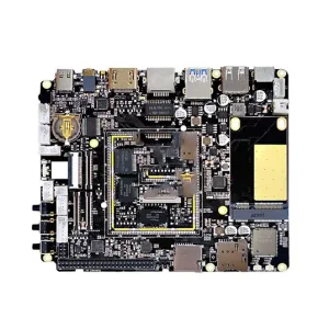
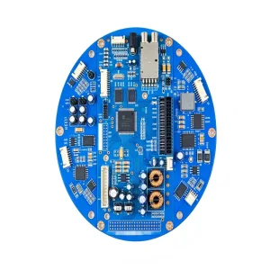
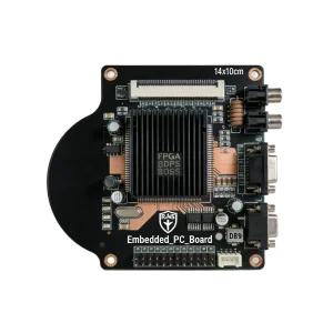
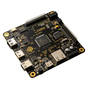
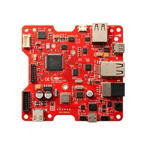
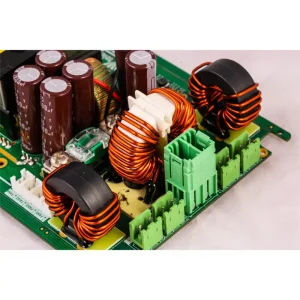
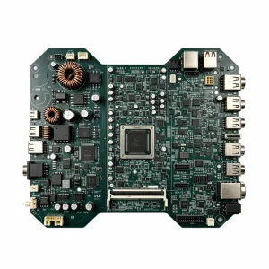
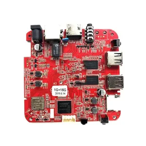
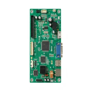
Explore real-world industrial deployments engineered under IATF 16949 and ISO 13485 quality frameworks, spanning green energy, clean mobility, IoT sensors, and high-speed telemetry.


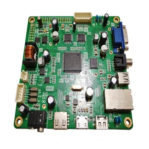
A rigorous engineering decomposition of Surface Mount Technology (SMT) vs. Surface Mount Device (SMD), multilayer interconnection dynamics, and the anatomy of high-reliability Printed Circuit Board Assembly (PCBA).
In modern electronics manufacturing terminology, SMT PCB Meaning encompasses far more than simply affixing microscopic components onto copper-clad laminate. At its baseline, SMT (Surface Mount Technology) denotes the automated manufacturing methodology wherein electronic components are placed directly onto the planar pads of a printed circuit board, eliminating the parasitic inductance, thermal dissipation bottlenecks, and mechanical space constraints typical of legacy Through-Hole Technology (THT).
To fully appreciate the term, one must distinguish between SMT (the assembly methodology), SMD (Surface Mount Device) (the active or passive component packaged for planar landing, such as 01005 passives, QFNs, BGAs, and CSPs), and PCBA (Printed Circuit Board Assembly) (the fully realized functional system once soldering, inspection, testing, and firmware integration are completed). A "High-Quality SMT PCB Service" refers to the holistic, closed-loop industrial ecosystem wherein bare board fabrication (rigid, flex, rigid-flex, metal-core, or high-density interconnect HDI), high-speed component placement, metallurgical reflow soldering, and automated optical/X-ray verification operate under rigorous statistical process control (SPC).
When hardware developers evaluate high-quality SMT PCB meaning, they demand sub-micron solder deposition precision, controlled impedance matching (±5% tolerance), micro-via aspect ratio integrity, thermal pad voiding rates below 10-15% on high-power thermal lands (such as exposed pads of MOSFETs or automotive LED drivers), and zero coplanarity deviation across high-pin-count Ball Grid Arrays.
THT requires drilled lead holes traversing every inner layer, consuming routing channels. SMT enables double-sided high-density population, minimizes lead inductance, elevates signal transmission speeds past 25 Gbps, and slashes total assembly weight by up to 60%.
High-quality SMT requires specialized substrate chemistry. From standard FR-4 (Tg 140°C to 170°C+) to Rogers ceramic substrates for RF radar, polyimide for dynamic flex circuits, and insulated metal substrates (IMS) for high-lumen illumination.
SMT joints rely on SAC305 (Sn96.5Ag3.0Cu0.5) lead-free alloys or specialized low-temperature bismuth-tin mixes. Precise reflow profile management prevents thermal shock, intermetallic compound (IMC) brittleness, and tombstoning.
From 01005 discrete chips to ultra-fine 0.35mm pitch WLCSP and 1500+ ball FC-BGA packaging. Automated placement accuracy reaches ±0.015mm with closed-loop optical fiducial alignment and intelligent tape feeders.
Eliminating multi-vendor friction through a unified manufacturing pipeline with complete lot traceability, strict incoming quality gates, and automated test fixtures.
Automated Gerber & BOM scrutiny identifying footprint mismatches, solder-mask clearance issues, and thermal balance anomalies before stencil cutting.
Global component procurement via authorized franchised distributors and vetted suppliers. 100% incoming XRF anti-counterfeit & solderability audits.
High-precision drilling, laser direct imaging (LDI), automated optical inspection (AOI) on inner layers, and controlled impedance etching.
Fully automated screen printing with 3D-SPI, high-speed chip shooters, multi-zone N2 convection reflow ovens, and precise selective soldering.
In-line 3D Automated Optical Inspection accompanied by 2D/3D X-Ray Inspection for hidden BGA/QFN solder joints, bridging, and void quantification.
On-board firmware flashing, in-circuit testing (ICT), customized functional test jigs (FCT), environmental burn-in, and RF signal calibration.
Automated conformal coating, potting, ultrasonic enclosure welding, CNC wire harnessing, final retail box build packaging, and air/sea dispatch.
Why Tier-1 global OEMs, venture-backed hardware startups, and mission-critical engineering firms consolidate high-mix SMT production in Shenzhen.
Selecting a China SMT PCB factory in Shenzhen is not merely a wage-arbitrage calculus; it is a structural strategic advantage rooted in industrial cluster density. Within a 30-kilometer radius in Shenzhen's Bao'an and surrounding industrial corridors, a hardware engineering team has immediate, physical access to raw copper laminates, specialized solder chemistries, specialized laser-cut stencils, custom plastic tooling, high-precision CNC metal enclosures, silicone seals, and every passive/active electronic component cataloged in global supply databases.
While Western or localized regional assembly shops often face a 3-to-6 week procurement hurdle for passive reels or custom PCB substrates, a Shenzhen-based facility like STHL completes component arrival, stencil calibration, DFM modifications, and trial surface mount line startup in as little as 24 to 48 hours. This dramatic velocity reduction shortens the New Product Introduction (NPI) timeline from quarters to weeks, granting international clients an insurmountable time-to-market advantage.
| Evaluation Parameter | Certified China SMT Factory (STHL) | Typical Western EMS Contract Manufacturer | Fragmented Multi-Vendor Sourcing |
|---|---|---|---|
| BOM Turnaround & Component Availability | Immediate access to local stockists + 100+ global franchised partners; 24h rapid BOM sourcing | 4 to 8 weeks standard procurement cycle; frequent spot market premiums | High logistical overhead; individual supplier markups and shipment delays |
| NPI Rapid Prototyping Lead Time | 24 to 72 hours quick-turn SMT line readiness with dedicated NPI engineering | 3 to 5 weeks standard lead time for small-batch validation | Unpredictable; dependent on bare board fab shipping across borders |
| NRE Tooling & Setup Surcharges | Ultra-low or zero setup fees; cost-neutral laser stencils and test jigs | Substantial engineering non-recurring engineering (NRE) charges ($2k - $8k+) | Repeated fixture costs at every disparate fabrication vendor |
| Minimum Order Quantity (MOQ) | Strict No MOQ policy (1 piece to 1,000,000+ units seamlessly transitioned) | Rigid MOQs typically enforced (500 to 5,000 units minimum) | Inconsistent MOQs across each discrete sub-contractor |
| Quality Architecture & Traceability | IATF 16949, ISO 13485, ISO 9001 certified; centralized MES barcoding per board | High compliance standards, but often cost-prohibitive for high-mix/low-volume | Fragmented traceability; prone to inter-vendor finger-pointing when faults arise |
Anticipating the structural pivots toward miniaturization, artificial intelligence-driven inspection, thermal dissipation extremes, and sustainable circular manufacturing.
Traditional threshold-based AOI is yielding to deep convolutional neural networks (CNNs) capable of distinguishing harmless flux residues from true micro-cracks or solder bridges. Closed-loop feedback between 3D-SPI and stencil printers enables autonomous solder volume compensation on the fly.
The transition toward Silicon Carbide (SiC) and Gallium Nitride (GaN) power semiconductors demands exceptional thermal junction management. SMT lines now utilize vacuum reflow soldering to suppress voiding below 5%, paired with direct copper bonding (DCB) substrates.
As wearables and military IoT devices shrink, SMT processes are migrating beyond 0201 packaging toward 008004 components and bare die integration directly into inner substrate cavities (Embedded Component Technology - ECT), drastically eliminating surface area usage.
From extreme thermal cycles in desert photovoltaic farms to the life-critical telemetry of clinical operating theaters, each mission demands customized assembly tolerances.
Engineered under IATF 16949 standards, automotive PCBA must withstand continuous vibrations, wide operating temperatures (-40°C to +125°C), and high voltage spikes in onboard chargers (OBC) and battery management systems (BMS).
Governed by ISO 13485, healthcare electronics demand absolute signal fidelity, biocompatibility safety clearances, and pristine cleanliness standards to avoid leakage currents in sensitive analog bio-sensor interfaces.
Solar photovoltaic power monitors, micro-inverters, and wind turbine pitch controllers face relentless UV exposure, high thermal cycling, and lightning surges. Thick-copper PCB layers (up to 4oz+) are expertly soldered without delamination.
High-speed networking cards, optical transceivers, and edge compute boxes rely on micro-vias, back-drilled differential pairs, and controlled dielectric properties ensuring signal integrity over 112G PAM4 communication protocols.
A procurement playbook for technical sourcing directors, supply chain VPs, and engineering executives evaluating offshore PCBA manufacturing partners.
Procuring electronic manufacturing services globally introduces a classic trilemma: achieving uncompromising military or automotive grade reliability while compressing production cycles and defending margins against inflationary component volatility. Sophisticated international buyers no longer prioritize the lowest bill of materials quote on paper; they look for Total Cost of Acquisition (TCA) and systematic risk mitigation.
The most crippling hidden costs in hardware programs stem from post-assembly field failures, counterfeit component batch contamination, and communication breakdowns during engineering change orders (ECO). By anchoring production in a vertically integrated factory like STHL that guarantees non-disclosure agreement (NDA) protections before engineering review, provides in-house XRF spectrometry for metallurgy checks, and maintains automated Manufacturing Execution Systems (MES) logging every reflow temperature curve, global enterprises transform contract manufacturing from a volatile liability into a defensible competitive moat.
STHL executes legally binding NDAs prior to RFQ review. Firmware is flashed inside secure, isolated local networks with zero external cloud exposure, protected by encrypted hex loaders.
Our engineering division continuously audits BOMs to recommend pin-compatible alternate passives and ICs with guaranteed supply horizons, mitigating obsolete lifecycle (EOL) risks.
Global buyers can audit our cleanrooms, ESD floor dissipation, and SMT lines remotely via high-definition 360° interactive VR platforms or schedule on-site factory verification in Bao'an, Shenzhen.
Independent third-party audits verify our operational adherence to the world’s most stringent automotive, healthcare, and industrial standards.

Automotive Quality Defect Prevention
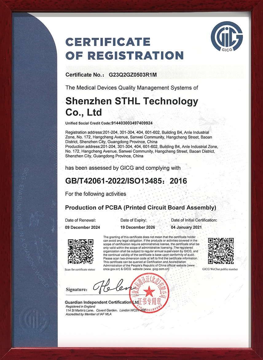
Medical Device Traceability Standard

Quality Management System Certification

Environmental Compliance & Sustainability











Comprehensive engineering insights clarifying design rules, cost variables, stencils, inspection, and supply-chain risk mitigation.
Explore our turnkey PCBA capabilities across mission-critical networking, redundant power conversion, precision inertial measurement units, and intelligent lighting systems.
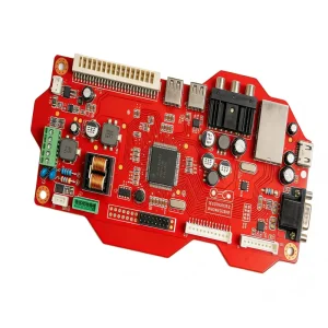
Send your Gerber package, Bill of Materials (BOM), and assembly criteria today. Our engineering team returns a complete DFM/DFA assessment, component optimization audit, and competitive turnkey quote within 24 hours.