Explore our turnkey PCBA assemblies built under continuous inline automated optical, X-ray, and functional electrical testing to ensure IPC-A-610 Class 3 compliance across consumer, commercial, and industrial markets.
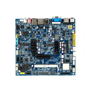
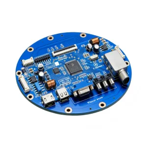
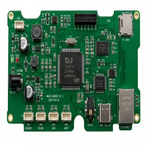
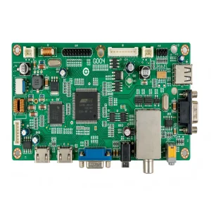
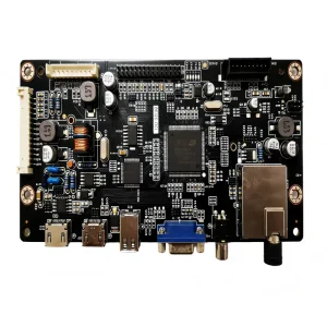
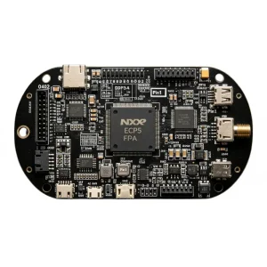

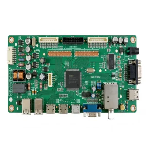
As surface-mount component packages shrink below 01005 (0402 metric) chips and ultra-fine-pitch Ball Grid Arrays (BGA) and Quad-Flat No-Leads (QFN) feature ball pitches below 0.35 mm, surface-mount technology (SMT) can no longer rely on sample visual audits. Modern high-reliability electronics demand a quantitative, mathematical verification framework that monitors every micromillimeter of solder deposition, component placement co-planarity, reflow thermal profiles, and electrical continuity.
Shenzhen STHL Electronics Co., Ltd. (operating since 2006 from Bao'an, Shenzhen) has built an end-to-end, multi-tier SMT testing architecture. Combining 7 high-speed Yamaha and Panasonic SMT lines, 2 automated DIP/THT lines, 2 dedicated functional test lines, and 2 box-build assembly cells, our 220+ workforce and 50+ engineers safeguard every printed circuit board assembly through rigorous statistical process control (SPC).
| SMT Inspection Tier | Key Physical Metric Checked | Defect Prevention Target |
|---|---|---|
| 3D SPI Inline | Paste volume (±10%), height, area, bridge risk | Eliminates >70% of downstream soldering defects |
| Pre-Reflow AOI | Part presence, orientation, theta rotation, offset | Prevents reflow consolidation of placement errors |
| Post-Reflow 3D AOI | Meniscus height, wetting angle, solder bridges, lift | Ensures IPC-A-610 Class 2 & 3 solder joints |
| 3D AXI (X-Ray) | Voiding %, solder ball coplanarity, HIP, barrel fill | Guarantees hidden joint integrity beneath BGA/QFN |
| In-Circuit Test (ICT) | Open/short nets, component value drift, RLC tolerance | Catches wrong reels, ESD degradation & cracked MLCC |
| FCT & Boundary Scan | Dynamic functional logic, firmware execution, bus speed | 100% operational verification prior to packaging |
Explore how industrial artificial intelligence, closed-loop M2M communications, and automated cloud SPC redefine PCBA quality assurance over the next decade.
Traditional SMT lines isolate the stencil printer, pick-and-place, reflow oven, and inspection systems. At STHL, our 3D SPI continuously feeds volumetric data back to our automated Yamaha paste printers. If paste deposition drifts by ±3 microns, the printer automatically executes dry-wipe stencil cleaning, squeegee pressure leveling, and offset recalibration without human intervention, arresting defect generation before solder reflow begins.
Optical inspection historically suffered from high "false call" rates due to component specular reflections, varying solder luster, and silkscreen font deviations. STHL has deployed AI deep learning inference models trained on over 5,000,000 empirical solder joint defect datasets. Our systems distinguish benign optical variations from genuine micro-cracks, cold solder joints, Head-in-Pillow (HiP) phenomena, and partial wetting anomalies with >99.98% accuracy.
With 5G-Advanced, 6G millimeter-wave, and edge AI compute PCBA accelerating, parasitic capacitance and trace impedance tolerances are razor-thin. Our engineering roadmap integrates automated vector network analysis (VNA) at inline test fixtures, coupled with digital twin simulation software. This enables thermal stress mapping, dynamic signal integrity verification, and predictive component MTBF analysis before the physical board ships.
A single test standard cannot satisfy the diverse compliance environments of different industrial sectors. STHL tailors its SMT test matrix to the exact regulatory risk profiles of mission-critical hardware.
Zero-defect mandate for ADAS modules, powertrain controllers, battery management systems (BMS), and telematics. Implementation of 100% 3D AXI on power semiconductors, temperature cycling (-40°C to +125°C), thermal shock stress testing, and component reel trace mapping to eradicate automotive field recalls.
Specialized validation protocols for surgical instruments, patient vitals monitoring, and diagnostic imaging PCBA. Complete component serialization, bio-compatibility conformal coating thickness audits, automated boundary-scan JTAG vector analysis, and non-destructive dielectric breakdown safety testing.
Tailored for programmable logic controllers (PLCs), variable frequency drives (VFD), and robotic sensors subjected to continuous mechanical vibration, ambient thermal variance, and electrical transients. High-load burn-in screening at 60°C for 72 hours, bed-of-nails in-circuit testing, and conformal coat UV luminescence inspection.
Uncompromising durability for navigation computers, EFIS avionics, and radar modules. Multi-axis high-resolution X-ray computed tomography for through-hole barrel solder fill (>75%), ion chromatography ionic cleanliness validation, and conformal coating bubble/delamination microscopics.
Global original equipment manufacturers (OEMs) operate in an era where design cycles have compressed from years to months, while component market volatility can disrupt production overnight. Located in the heart of Bao'an, Shenzhen—the global epicenter of microelectronics manufacturing—STHL leverages unprecedented regional supply chain density.
Our Factory 4.0 infrastructure connects our automated component warehouse with over 100 verified franchise distributors (Arrow, Avnet, Digi-Key, Mouser, STMicroelectronics, Microchip, and TDK). Using automated barcode and RFID lot-level tracing, incoming components undergo XRF spectroscopic verification to authenticate metallurgy, solderability dipping tests, and counter-deception decapsulation sampling before feeder loading.
| Manufacturing Dimension | STHL Shenzhen Smart Factory | Typical Fragmented EMS Provider |
|---|---|---|
| BOM Procurement Lead Time | 3 - 7 Business Days (Direct franchise agent ecosystem) | 3 - 6 Weeks (Brokered supply chain layers) |
| DFM & DFT Feedback Latency | < 24 Hours by dedicated engineering team | 3 - 5 Days with frequent delays |
| Testing Traceability | 100% Barcode MES Serialization (Retained 5 years) | Manual paper logbook or batch-only records |
| Inline SMT Line Speed | 0.025 sec/chip (Multi-head high-speed pick & place) | Legacy semi-manual or older generation SMT lines |
| Minimum Order Quantity (MOQ) | No MOQ (Full prototype-to-volume support) | Strict high MOQ requirement (500+ units minimum) |
Overseas procurement teams require absolute confidence regarding intellectual property confidentiality, regulatory adherence, and frictionless logistics. Here is how STHL safeguards global contracts.
Customer proprietary Gerber files, firmware hex binaries, and schematics are housed on encrypted, air-gapped on-premise servers with restricted role-based clearance. STHL signs internationally enforceable NDAs prior to RFQ document reviews, guaranteeing that proprietary innovations remain confidential across 90+ global export destinations.
Our manufacturing and testing lines operate under rigorous international certifications audited continuously by certified independent registrars: IATF 16949 (Automotive defect prevention), ISO 13485 (Medical device quality management), ISO 9001 (Standard operational management), and ISO 14001 (Environmental stewardship).
STHL manages express customs clearance and direct DDP (Delivered Duty Paid), FOB, or EXW shipments to hardware innovators across the USA, Germany, Italy, UK, Poland, Brazil, New Zealand, and beyond. Utilizing ESD vacuum packaging, humidity indicator cards, and anti-vibration crating, assemblies arrive factory-fresh.
Purchasing directors and VP of Engineering leaders balance BOM budget constraints with catastrophic product failure risks. How does investing in a disciplined SMT testing process reduce overall lifecycle costs?
Fixing a soldering anomaly at the SMT paste printer via 3D SPI costs less than $0.10. Detecting the same anomaly at post-reflow AOI costs $1.00. Finding it at functional ICT costs $10.00. Discovering it at finished box-build costs $100.00, while a field return can exceed $1,000.00. Our rigorous front-end SMT testing gates truncate downstream scrap and customer warranty liabilities.
Before launching stencil fabrication or PCB panelling, STHL's 50+ engineers analyze your Gerber, BOM, and centroid files for Design for Manufacturability (DFM) and Design for Testability (DFT). We verify fiducial placement, test point access pitches (≥0.8 mm for reliable bed-of-nails contact), shadow effect clearance for reflow convective heat transfer, and pad geometry optimization.
Subcontracting PCB fabrication to vendor A, component procurement to vendor B, SMT assembly to vendor C, and test programming to vendor D creates hand-off errors, double freight markups, and fingerprint deflection when defects arise. STHL accepts complete single-source accountability under one integrated roof.
Detailed technical responses addressing the real-world manufacturing, test engineering, and supplier qualification inquiries faced by global hardware developers.
Empirical manufacturing studies prove that between 65% and 75% of all PCBA solder defects—such as bridges, tombstoning, and insufficient solder volume—originate during the solder paste printing step. 3D SPI evaluates solder deposition volumetrically before components are placed and reflowed. By catching irregular height, bridging, or insufficient volume on 0201/01005 pads or 0.4mm BGA pads before solder melts, boards can be cleanly washed and reprinted, eliminating permanent scrap and costly rework cycles.
Components with bottom-termination pads (BTC) like Ball Grid Arrays (BGAs) and QFNs cannot be inspected by optical line-of-sight cameras. STHL utilizes high-resolution 3D Automated X-ray Inspection (AXI) and high-magnification oblique-angle X-ray systems. Our algorithms analyze solder ball co-planarity, Head-in-Pillow (HiP) anomalies, solder bridging, and compute voiding percentages across all thermal and signal pads to ensure voiding remains strictly under 10%–15% according to IPC-7095 Class 3 guidelines.
Flying Probe uses precision CNC mechanical arms to probe test points and component leads directly without requiring customized physical bed-of-nails fixtures. This makes FPT exceptionally cost-effective and agile for prototypes and low-to-medium runs (zero tooling charge). Conversely, ICT uses a custom bed-of-nails fixture capable of contacting thousands of test points simultaneously in seconds, making it the industry standard for high-volume automotive and consumer runs despite initial fixture NRE.
We purchase components solely from authorized direct distributors (Arrow, Avnet, Digi-Key, Mouser, verified component factories) with full certificates of conformance (CoC). Our incoming quality control (IQC) laboratory performs X-ray inspection to check internal die wire bonding, XRF spectroscopy to confirm RoHS/lead-free compliance, and solderability tests under IPC/JEDEC J-STD-002 to ensure aging reels do not present wetting risks.
To deliver rapid, accurate DFM and quote feedback within 24 hours, our engineering team requires: (1) ODB++ data or RS-274X Gerber files with drill data; (2) Detailed Bill of Materials (BOM) containing manufacturer part numbers (MPN), reference designators, and package descriptions; (3) Pick-and-Place XY centroid coordinates file; and (4) Functional testing specifications or schematics outlining voltage rails, test vectors, and firmware flashing procedures.
Yes. We feature 2 dedicated functional testing production lines equipped with pneumatically actuated test fixtures, multi-channel oscilloscopes, dynamic signal generators, CAN bus analyzers, and automated flash programmers. Customers can either ship turnkey test fixtures to our Shenzhen factory or provide technical schematics and guidelines for our in-house engineering team to design, assemble, and validate custom FCT test beds locally.
We use 10-zone reflow ovens equipped with real-time KIC thermal profilers. Before production begins, thermocouples are attached to critical components (e.g., largest BGA, smallest 0201 chip, high-mass inductors, and connectors) to construct a bespoke thermal profile. We tightly govern soak zone delta-T, maintain ramp rates below 2.5°C/second to eliminate thermal shock, and ensure time-above-liquidus (TAL) meets exact solder alloy chemistry (typically 45-75 seconds for SAC305 at 217°C melting point).
For industrial and aerospace boards operating in harsh climates, STHL operates programmable environmental thermal chambers (-50°C to +150°C) and humidity stress chambers. We also provide automated robotic selective conformal coating (acrylic, polyurethane, silicone, or UV-cure) to protect assemblies from moisture, dust, salt spray, and corrosion, validated under UV blacklight inspection systems.
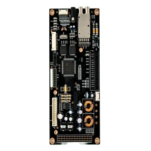
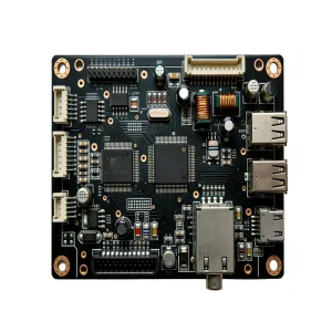
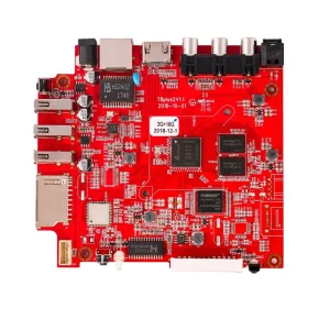
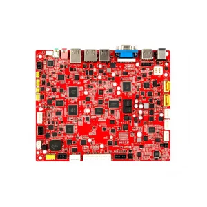
Demonstrating our deep manufacturing mastery across life-safety medical navigation, avionics electronic flight instrumentation, automotive braking, and precision industrial power supplies.
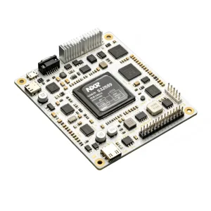

Send your Gerber RS-274X/ODB++ and BOM files directly to our engineering team in Bao'an, Shenzhen. Receive a confidential, comprehensive DFM/DFT analysis and competitive turnkey quotation within 24 hours.
