Engineered to IPC Class 2 and Class 3 benchmarks across medical, aerospace, automotive, and high-frequency communication infrastructures.


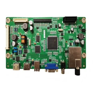
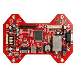
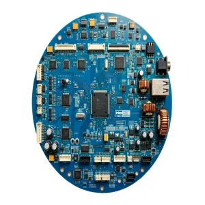
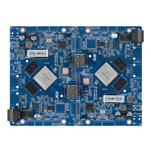
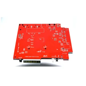

A systematic analysis distinguishing raw bare printed circuit boards from fully active, functional electro-mechanical assemblies.
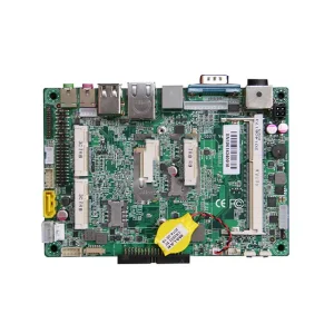
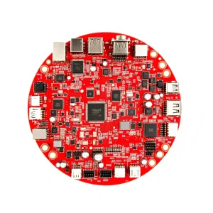
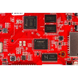
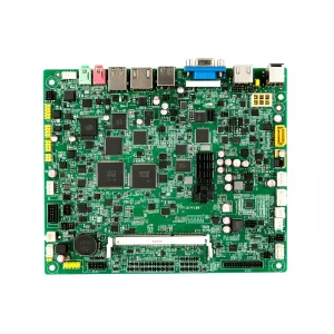
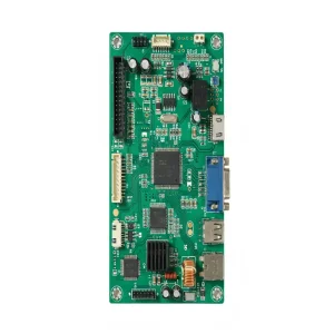
A bare Printed Circuit Board (PCB) is merely an unpopulated passive mechanical carrier made of woven fiberglass (FR-4, high-Tg), Rogers dielectric, or polyimide, layered with etched copper traces, micro-vias, and a protective solder mask. In contrast, a Printed Circuit Board Assembly (PCBA) is the finished, operational system realized after soldering active silicon dies, microcontrollers, passive pass-through components (01005 passives, ceramic capacitors), and high-pin-count Fine-Pitch Ball Grid Arrays (FBGA).
High-grade PCBA manufacturing relies on rigorous intermetallic compound (IMC) boundary engineering. Using RoHS-compliant SAC305 (Sn96.5Ag3.0Cu0.5) or specialized low-temperature bismuth-tin (Sn42Bi58) solder pastes, SMT engineers must tightly balance the liquidus phase (typically 217°C) with thermal mass dissipation across massive ground planes and delicate QFN packages, eliminating non-wetting, cold joints, and voiding under high-stress thermal cycling.
A contemporary PCBA is rarely an isolated entity. It represents an integrated system comprising High-Density Interconnect (HDI) Microvia substrates, rigid-flex transitions, edge-connector high-speed differential signal traces (supporting PCIe 5.0, USB4, and multi-gigabit Ethernet), embedded RF shields, thermal interface dissipation pads, and secure crypto-element hardware protection keys integrated directly on the motherboard substrate.
Navigating the systemic shifts in global electronic manufacturing: reshoring, nearshoring, regional specialization, and multi-hub resilience.
The Pearl River Delta remains the global epicenter for rapid NPI (New Product Introduction), turnkey BOM sourcing, and high-complexity SMT assembly. With instant access to major semiconductor distribution networks (Arrow, Avnet, Digi-Key, Mouser) and millions of raw component SKUs within a 30-kilometer radius, industrial factories achieve prototype turnaround in 24–48 hours, scaling seamlessly to multi-million-unit mass production.
Global procurement teams now mandate "China Plus One" risk mitigation strategies. Leading PCBA conglomerates maintain dual-hub operational footprints: high-complexity fabrication, SMT engineering, and automated testing clustered in automated Shenzhen centers, with localized assembly, final packaging, and tariff-optimized box build distributed across Southeast Asia (Vietnam, Malaysia, Thailand), Mexico, and Eastern Europe.
Component obsolescence and volatile allocation cycles (such as recent automotive micro-controller shortages) have transformed electronic procurement. World-class factories utilize AI-driven BOM lifecycle analyzers, directly linking engineering ERP systems with live silicon inventory to propose pin-to-pin drop-in replacements, Second Source options, and redesign-for-procurement strategies prior to production sign-off.
The convergence of artificial intelligence, high-frequency RF, and sub-micron packaging requires factories to evolve far beyond traditional pick-and-place lines.
As wearables and AI edge sensors compress volumetric envelopes, automated SMT lines deploy ultra-high-speed modular placers capable of mounting 01005 (0.4mm × 0.2mm) passives and 0.3mm pitch micro-BGA packages with ±20-micron placement repeatability.
Traditional 2D AOI inspection has surrendered to inline 3D Solder Paste Inspection (SPI) with phase-shift moiré fringe projection, combined with continuous 3D Automated X-ray Inspection (AXI) to identify internal BGA micro-voiding and non-wet-open defects.
System-in-Package (SiP) technology embeds passive resistors and active bare dies directly within the inner laminate layers of the PCB substrate, dramatically decreasing parasitics, suppressing EMI emissions, and liberating external surface mounting real estate.
Tier-1 factories adopt halogen-free laminates, zero-waste flux clean processes, and low-melting-point solder alloys (reducing reflow peak temperatures from 245°C to 180°C) to slash carbon emissions, comply with EU WEEE mandates, and prevent thermal warping.
A reference checklist for hardware engineering directors and strategic sourcing managers when qualifying candidate assembly partners.
| Evaluation Parameter | Standard Low-Cost Assembly | High-Reliability Tier-1 EMS | STHL Industrial Benchmark |
|---|---|---|---|
| Target Quality Standard | IPC-A-610 Class 1 (Commercial) | IPC-A-610 Class 2 / Class 3 | IPC-A-610 Class 3 / IATF 16949 / ISO 13485 |
| Min. Passive Placement | 0402 (1.0mm × 0.5mm) | 0201 (0.6mm × 0.3mm) | 01005 (0.4mm × 0.2mm) with ±20µm accuracy |
| Solder Inspection | Manual visual / basic 2D AOI | Inline 3D SPI + 2D AOI | Real-time Inline 3D SPI + High-res 3D AOI + 3D AXI |
| Thermal Profiling | Standard furnace presets | Thermal logger verification | Real-time 10-zone reflow curve with KIC profiling |
| Traceability Infrastructure | Batch-level paper records | Work-order barcode scans | MES lot/reel/die traceability down to reference designator |
| BOM Management | Manual broker purchasing | Authorized distributor sourcing | Direct franchise contracts (Arrow, Avnet, Microchip, ST) |
How an electronics assembly factory transitions digital files into robust, tested, and mission-ready industrial hardware.
Comprehensive checks across Gerber, ODB++, centroid, and BOM files to detect clearance, footprint, and thermal land issues.
Full-traceability component sourcing from franchise channels; incoming counterfeit inspection and moisture baking.
High-precision laser stencil solder printing, 3D SPI, multi-head component pick-and-place, and controlled 10-zone nitrogen reflow.
Rigorous inline 3D optical and X-ray inspection to guarantee complete solder fillet joint coverage and zero sub-BGA voiding.
Automated Through-Hole Technology (THT) insertion, robot selective soldering, and hand-soldering for mechanical interfaces.
In-Circuit bed-of-nails verification, automated flash firmware burning, boundary scan, and customized functional test (FCT) jigs.
Automated robotic conformal coating, potted encapsulation, full electromechanical box-build assembly, and ESD carton packing.
Full compliance paperwork, lot testing reports, certificate of conformities, and rapid bonded global freight delivery.
Tailored PCBA architectures designed to survive high-vibration, ionizing radiation, corrosive atmospheres, and prolonged thermal excursions.
Automotive PCBA demands zero-defect PPM production. From ADAS collision avoidance radars to high-voltage Battery Management Systems (BMS), manufacturing utilizes strict PPAP (Production Part Approval Process), APQP documentation, specialized underfills, and rigorous thermal shock testing from -40°C to +125°C.
Medical assemblies require end-to-end device history records (DHR) and absolute component traceability. Whether manufacturing patient monitors, surgical imaging platforms, or wearable insulin pumps, cleanroom assembly, validated conformal coating, and strict bio-burden mitigation are standard factory controls.
Harsh operating environments require thick copper (>3oz) boards, galvanic isolation barriers, transient voltage suppression networks, and selective silicone or polyurethane conformal coatings to safeguard electronics against conductive dust, humidity, and mechanical vibration.
Authoritative, engineering-level answers to critical inquiries regarding supplier qualification, assembly tolerances, and intellectual property.
Explore specialized industrial, environmental, energy, and precision computing PCB assemblies manufactured by certified factory partners.