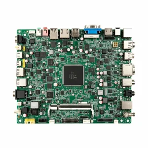
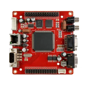
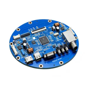
Explore our active manufacturing lines showcasing fine-pitch surface-mount technology, complex ball grid arrays, embedded IoT sensors, and high-density industrial control assemblies.
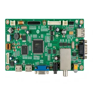
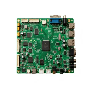
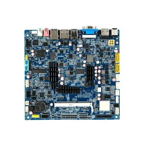
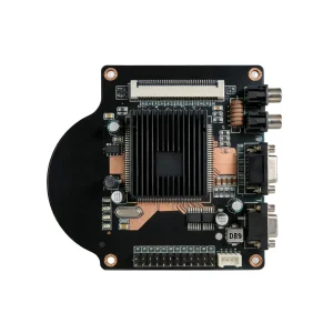
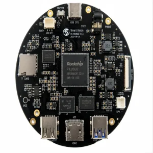
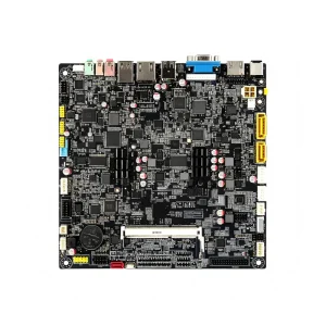
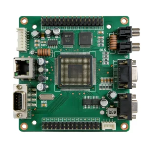
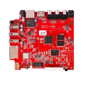
Ball Grid Array (BGA) and fine-pitch Micro-BGA (μBGA) packages represent the pinnacle of modern Surface Mount Technology (SMT). Delivering flawless interconnects requires deep thermodynamic profiling, metallurgical control, and automated X-ray inspection.
Thermal dynamic stresses during reflow often induce package warpage, leading to Head-in-Pillow (HiP) defects or bridged solder spheres. We implement strict dynamic shadow moiré interferometry measurements and customize reflow thermal profiles using 10-zone nitrogen convection ovens to keep substrate-package thermal gradients within ±2.0°C across large dies.
While IPC-A-610 Class 3 permits voiding up to 25% within solder balls, critical high-frequency, RF, and automotive applications demand much higher thermal conductivity. Utilizing vacuum-assisted reflow soldering systems, our Shenzhen manufacturing facility suppresses voiding below 8-10%, ensuring superior mechanical shear strength and optimal heat dissipation.
Fine-pitch BGAs (down to 0.3mm ball pitch) require electroformed or high-grade laser-cut stencils with nano-coating technology. We calculate precise area ratios (>0.66) and transfer efficiencies to prevent bridging and insufficient solder volume, combining SPI (Solder Paste Inspection) with real-time volumetric 3D laser profiling.
The convergence of edge AI computation, automotive autonomy, and ultra-compact connected devices requires high-layer-count HDI boards integrated with high-pin-count Ball Grid Arrays.
Modern System-on-Chips (SoCs), neural processing units (NPUs), and FPGAs deploy micro-ball arrays exceeding 1,500 pins. As AI inferencing transitions from remote hyperscalers to localized industrial IoT edge boxes and computer vision webcams, thermal density and impedance-matched signal paths become vital engineering prerequisites.
Powertrain microcontrollers, Battery Management Systems (BMS), and radar transceivers face extreme operational vibration and thermal cycling (-40°C to +125°C). BGA packages in automotive electronics require rigorous underfill application, lead-free SAC305 alloy validation, and compliance with stringent IATF 16949 production standards.
Next-generation patient monitors, surgical automation equipment, and portable ultrasound scanners utilize dense multi-layer rigid-flex boards populated with high-reliability BGAs. Medical electronics mandate full component-level MES lot traceability, ISO 13485 compliance, and complete protection against ionic contamination.
Shenzhen represents the epicentre of global hardware innovation. STHL leverages this dense geographical cluster to deliver unparalleled agility, rapid prototyping, and end-to-end component security.
Direct procurement channels through over 100 authorized agents and original component manufacturers provide verified access to more than 500,000 active part numbers. We protect builds against counterfeit components via certified testing labs and incoming X-ray fluorescence analysis.
Our dedicated engineering department of 50+ specialists reviews your Gerber, BOM, and centroid files before production. We assess via-in-pad plating, solder mask dams between BGA pads, trace escape routing, and thermal relief patterns to avoid costly engineering redesigns.
Equipped with 7 advanced automated SMT lines, 2 DIP/THT lines, 2 dedicated functional test lines, and 2 box-build assembly units. We accommodate high-mix low-volume (HMLV) pilot batches without MOQ constraints, scaling seamlessly into mass production runs.
Intellectual property protection is secured under rigorous Non-Disclosure Agreements prior to file handoff. Factory-wide MES (Manufacturing Execution System) assigns individual 2D data-matrix barcodes, tracking component reels, operator IDs, reflow profiles, and AXI data for complete lifecycle traceability.
BGA components provide the electrical performance, signal integrity, and package miniaturization required by high-complexity electronic assemblies across industries.
Compact smart home devices, agricultural soil detectors, and door/window sensors demand ultra-small footprints with minimal parasitic inductance. Utilizing 0.4mm micro-BGA microcontrollers and BLE/Wi-Fi SiP (System-in-Package) modules, we maximize battery life through ultra-low leakages and minimal thermal drift.
High-throughput PoE injectors, load balancers, and wireless edge communication equipment rely on high-speed multicore processors housed in flip-chip BGAs (FCBGA). Signal integrity analysis, differential impedance routing, and power distribution network (PDN) decouping capacitors ensure uninterrupted data throughput under full thermal load.
Continuous industrial operation requires robust resistance to mechanical shock and thermal extremes. Laboratory analyzers, automated testing jigs, and bench power supply controllers incorporate FPGA and DSP BGAs requiring selective underfill, automated optical inspection, and rigorous functional bed-of-nails validation.
Our Shenzhen manufacturing facility is outfitted with advanced Japanese high-speed surface mounters, nitrogen convection ovens, and 3D automated X-ray inspection equipment.
| Manufacturing Parameter | Standard Capability | Advanced / High-Density Capability | Inspection & Verification Methodology |
|---|---|---|---|
| BGA Ball Pitch | 0.50 mm (19.7 mil) | 0.30 mm (11.8 mil) / Micro-BGA | 3D Solder Paste Inspection (SPI) & 3D AXI |
| Min Component Package | 0201 (Imperial) / 0603 (Metric) | 01005 (Imperial) / 0402 (Metric) | High-resolution optical alignment & AOI |
| Max Board Dimensions | 510 mm × 460 mm | 610 mm × 510 mm | Custom conveyor carrier systems |
| Board Thickness Range | 0.4 mm – 3.2 mm | 0.2 mm – 6.0 mm (Rigid-Flex & Backplane) | Laser micro-height measurement sensors |
| PCB Layer Count | 2 – 16 Layers | Up to 32 Layers / Any-Layer HDI (ELIC) | Micro-sectioning & TDR Impedance Testing |
| Solder Sphere Alloys | SAC305, SAC387 (Lead-Free) | Sn63Pb37 (High-Rel), Low-Temp LTS (Bi-Sn) | X-Ray Fluorescence (XRF) alloy verification |
| Solder Voiding Limit | < 15% (IPC-A-610 Class 2) | < 8-10% (IPC Class 3 & Vacuum Reflow) | Off-axis high-resolution 3D CT X-Ray |
| Underfill Dispensing | Manual pneumatic dispense | Fully automated jet-valve dispensing with heated stage | Acoustic micro-imaging & shear testing |
| BGA Rework Capability | Hot air rework station | Computerized split-beam optical rework system | Pre-heat profiling, laser thermal feedback |
As semiconductor packaging embraces heterogenous integration, chiplets, and substrate-level convergence, our manufacturing roadmap ensures complete readiness for next-decade electronics.
To eliminate high-speed memory bus bottlenecks, mobile and wearable architectures mount memory BGAs directly atop application processors. PoP assembly requires micron-accurate two-stage flux dipping, precise dual-level reflow thermal profiling, and 3D radiographic cross-verification to prevent lower-level joint collapse.
Traditional subtractive PCB etching limits trace widths and spacings to 50/50 μm. Moving toward Modified Semi-Additive Processes (mSAP), our fabrication lines achieve ultra-fine 25/25 μm geometries, allowing direct fanout for high-density micro-BGAs (<0.35mm pitch) without requiring expensive stacked microvia escalation.
By connecting high-speed 3D SPI, pre-reflow AOI, post-reflow AOI, and transmission 3D X-ray systems into a centralized neural network, our production line automatically adjusts stencil print pressure, blade angles, and pick-and-place XY offsets in real time, preventing defects before they occur.
Our facility operates under rigorous international quality management protocols, ensuring that your mission-critical designs comply with worldwide regulatory and functional mandates.
Certified automotive quality management system guaranteeing continuous defect prevention, severe thermal stress tolerance, and full tier-1 automotive supply chain compliance.
Strict controls governing medical device manufacturing, bio-compatibility assurance, static ESD control, and end-to-end device history records (DHR).
Comprehensive standard operating procedures for quality consistency, ERP-integrated procurement, sustainable green production, and safe chemical management.
Trained and certified IPC assembly specialists ensuring all solder joints, heel fillets, BGA void thresholds, and cleanliness levels satisfy high-reliability industrial benchmarks.
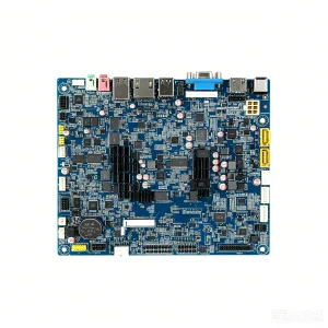
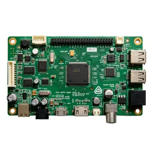
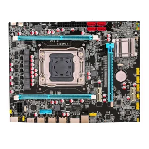
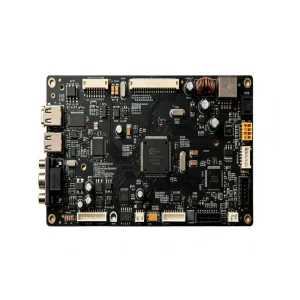
From complex industrial load balancers to critical battery management systems and security scanners, review our specialized PCB assembly production capabilities.

Detailed engineering answers to the most frequent technical inquiries presented by hardware designers, component procurement leads, and quality audit teams.
