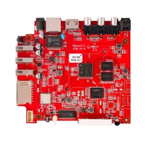
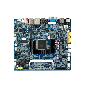
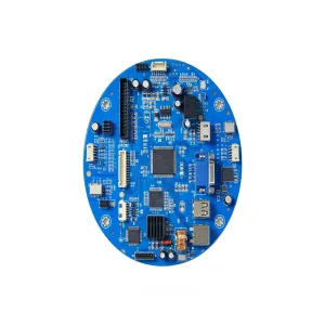
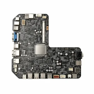
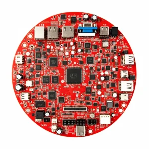
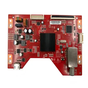
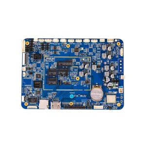
Engineered to deliver signal integrity, thermal dissipation, and long-term operating durability across industrial instrumentation, optical communications, and IoT platforms.
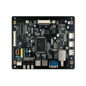
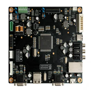

Resolving thermal density, signal degradation, and EMI/EMC compliance across 4- to 48-layer high-density interconnect (HDI) substrates.
In modern electronic systems design, multi-layer printed circuit boards (Multi Circuit Boards) serve as the fundamental nervous system and physical bedrock for high-performance computing, aerospace communication, automotive ADAS, and energy infrastructure. As semiconductor fabrication nodes advance toward sub-3nm geometries, silicon packages demand unprecedented routing density, sub-mil trace and space tolerances, and uncompromising power distribution network (PDN) stability. For tier-1 original equipment manufacturers (OEMs) and original design manufacturers (ODMs), partnering with an experienced OEM Multi Circuit Boards Manufacturer is not merely a purchasing transaction; it is an integrated engineering collaboration that dictates operational reliability, production yield, and time-to-market.
The manufacturing complexity of multi-layer assemblies increases exponentially with each added dielectric and copper layer. From standard 4-layer and 6-layer FR-4 substrates up to sophisticated 32+ layer backplanes incorporating sequential electrochemical lamination, blind/buried micro-vias, and copper-filled via-in-pad (VIPPO) structures, each fabrication phase presents strict physical and chemical challenges. A single micro-void in a copper plating barrel, a miscalculated dielectric constant ($\epsilon_r$), or an uncalibrated thermal coefficient of expansion (CTE) can cause delamination under lead-free reflow thermal shocks peaking at 260°C.
Utilizing laser direct imaging (LDI) and sequential build-up (SBU) technologies (1+N+1 to 4+N+4) to enable 0.35mm pitch fine-pitch ball grid arrays (BGA). Every via-in-pad is planarized, capped, and electroplated with pure copper to guarantee coplanarity and prevent solder migration.
Engineered dielectric thickness with low-loss laminates (Rogers RO4350B, Panasonic Megtron 6, Isola 370HR). Rigorous TDR (Time-Domain Reflectometry) testing verifies differential ($100\Omega \pm 5\%$) and single-ended ($50\Omega \pm 7\%$) impedance compliance across GHz frequency envelopes.
Mitigating localized junction heat through embedded heavy-copper inner layers (up to 6oz), metal-core substrates (aluminum/copper base), and strategic thermal via arrays with conductive epoxy backfills to maintain junction temperatures well within safe semiconductor thresholds.
Strategic bill-of-materials (BOM) management, counterfeit mitigation, and rapid qualification systems designed for frictionless OEM deployment.
The global printed circuit board assembly market has transitioned from purely low-cost outsourcing to a model demanding complete supply chain resilience, transparent traceability, and end-to-end risk management. Global OEM buyers—spanning North America, the European Union, Japan, and the APAC region—continually balance component obsolescence, geopolitical trade barriers, and extended lead times for active semiconductors. As an established Multi Circuit Boards Manufacturer based in Shenzhen's Bao'an electronics cluster, our production infrastructure integrates real-time API links with worldwide authorized distributors (Arrow, Avnet, Digi-Key, Mouser, Future Electronics) alongside audited domestic component fabrication hubs.
By leveraging an engineering team with over two decades of localized expertise, our front-end operations provide immediate BOM risk assessments. We identify "single-source" chips, microcontrollers nearing End-of-Life (EOL), and passive components with excessive lead times before factory tooling begins. Our proactive Design-for-Procurement (DFP) methodology suggests pin-compatible, drop-in alternatives, guaranteeing uninterrupted assembly flow while avoiding multi-month delays.
| Evaluation Parameter | Standard PCB Assembler | STHL OEM Multi Circuit Board Manufacturing | Engineering Value Delivered |
|---|---|---|---|
| Layer Count Feasibility | 1 to 8 Layers (Rigid FR-4 Only) | 2 to 48+ Layers (Rigid, Flex, Rigid-Flex, Metal-Core, Rogers) | Max Architectural Density |
| Component Traceability | Batch/Lot Level Receiving | Full MES Lot-to-Serial Traceability (Every reel & feeder logged) | Aerospace & Automotive Grade |
| Solder Joint Inspection | 2D Optical Inspection (AOI) | Inline 3D SPI + 3D AOI + High-Resolution 3D AXI (X-Ray) | Zero BGA Voiding Guarantee |
| Minimum Order Quantity | High MOQ (500-1000 pcs) | No MOQ (1 pc Quick-Turn Prototype to 100k+ Production) | Rapid Validation to Mass Scale |
| Impedance Simulation & Test | Theoretical Polar Si8000 only | Polar Si9000 Verification + TDR Physical Coupon Coupon Test | Guaranteed $Z_0$ Match |
Operating under stringent IATF 16949, ISO 13485, and ISO 9001 quality systems to support seamless cross-border deployment.
Deploying OEM multi circuit boards into international markets requires rigorous adherence to regional safety, electromagnetic, and environmental directives. Electronic modules destined for medical applications, high-reliability automotive powertrain units, or grid-tied photovoltaic monitoring equipment cannot afford intermittent cold solder joints or electrochemical migration under high humidity. Our cleanroom manufacturing plant operates in full compliance with IPC-A-610 Class 2 and Class 3 workmanship standards, governed by certified on-staff IPC trainers.
Specialized APQP (Advanced Product Quality Planning), PPAP Level 3 documentation, FMEA defect analysis, and 100% automated optical tracking designed for body control modules (BCM), EV battery management, and telematics units.
Controlled cleanroom environments, electrostatic discharge (ESD) flooring per ANSI/ESD S20.20, full device history record (DHR) tracking, and bio-compatible conformal coating application to ensure human-life safety in clinical monitors.
100% lead-free soldering verification (SAC305 / SAC0307 alloys), raw material XRF screening, halogen-free board construction, and UL 94V-0 flammability certification ensuring unrestricted entry into North American and EU jurisdictions.
How our multi circuit assemblies operate continuously in demanding, hostile real-world electrical and thermal conditions.
Integrated inside string inverters, battery management systems (BMS), and power optimizers. Multi-layer PCBA layouts isolate high-voltage switching noise from low-voltage microcontrollers, surviving ambient swings from -40°C to +85°C.
Employing low-loss Rogers hydrocarbon ceramic laminates paired with multi-layer FR-4 hybrids. Precision RF shielding cans, microstrip line impedance tuning, and automated pick-and-place precision for compact GNSS tracking systems.
Multi circuit boards engineered for gas leak detection, optical transceivers, and perimeter surveillance. Assemblies undergo automated conformal coating (acrylic or silicone) to resist corrosive airborne sulfur, moisture, and chemical vapor.
Integrating AI-driven automated optical defect inspection, embedded passive components, and ultra-low dielectric dissipation factors.
As computing requirements migrate to edge AI devices, the traditional boundaries between silicon packaging and PCB fabrication continue to converge. The roadmap for leading Multi Circuit Boards Manufacturers incorporates advanced substrate-like PCB (SLP) architectures featuring trace geometries narrower than 25/25 microns, mSAP (modified Semi-Additive Process) chemistries, and embedded active silicon dies within core dielectric laminations.
Furthermore, our manufacturing lines integrate artificial intelligence directly into the surface-mount technology (SMT) flow. Deep-learning neural networks cross-correlate 3D Solder Paste Inspection (SPI) volume measurements with post-reflow 3D Automated Optical Inspection (AOI) results. This closed-loop feedback loop automatically adjusts stencil printing parameters, squeegee pressure, and component pick offsets in real-time, driving defect rates down toward single-digit Parts Per Million (PPM).
Transitioning from subtractive chemical copper etching to modified semi-additive processes, unlocking razor-sharp rectangular trace cross-sections down to 20μm width for 112 Gbps PAM4 high-speed serial signaling.
Embedding passive capacitive layers and thin resistive foil directly inside the inner core laminates, freeing up critical surface real estate on outer layers while dramatically lowering parasitic inductance in high-speed microprocessors.
Pioneering low-temperature soldering (LTS) alloys that reduce peak reflow temperatures by 50°C, combined with 100% bio-based flux formulations, water-recycling closed-loop wash systems, and halogen-free laminates.
In-depth responses to assist component procurement directors, quality engineers, and hardware architects in qualifying our multi circuit manufacturing ecosystem.
Engineered for mission-critical power conversion, extreme environmental sensing, automotive chassis systems, and intelligent IoT controllers.
Upload your Gerber files and Bill of Materials for a comprehensive engineering assessment. Receive detailed DFM/DFA feedback, stackup impedance validation, and transparent volume pricing within 24 hours under NDA protection.