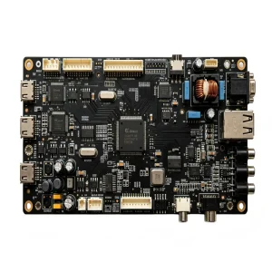
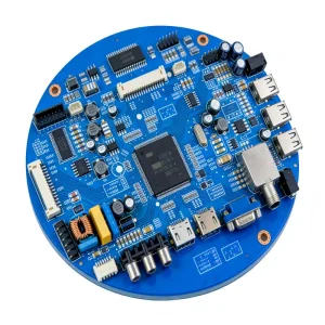
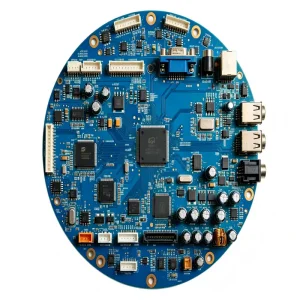
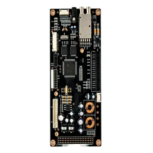
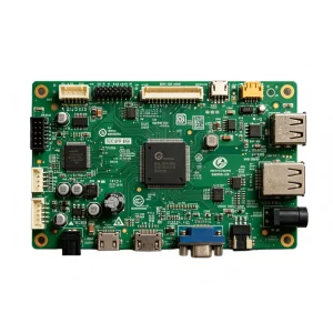
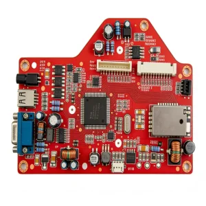
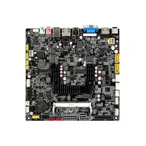
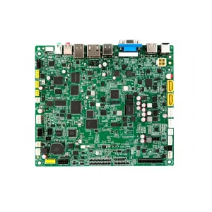
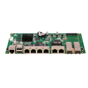
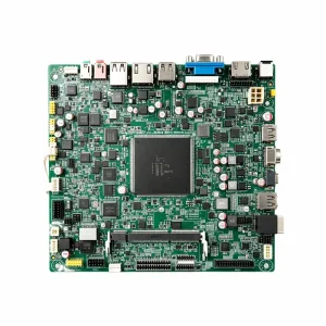
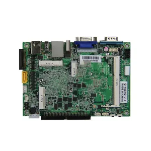
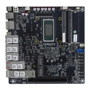
Explore production-grade assemblies built to strict IPC Class 2/3 criteria, ranging from smart-edge IoT units to high-density automotive domain controllers.
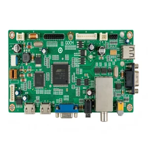
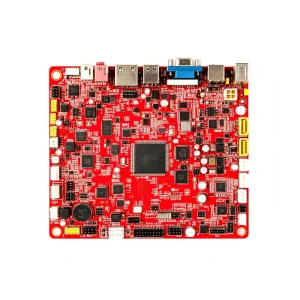
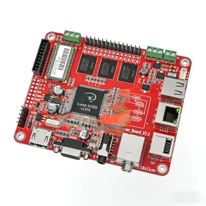
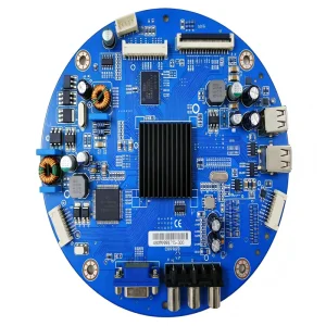
Electronic Manufacturing Services (EMS) have evolved past basic solder-paste application. Today's commercial ecosystem demands end-to-end design for manufacturability (DFM), deep supply chain redundancy, and zero-defect thermal execution.
Integrating pre-fabrication DFM analysis, high-speed automated placement, and in-line profiling. Sourcing raw materials directly through factory authorizations prevents multi-tier broker friction.
State-of-the-art 10-zone nitrogen-purged reflow ovens ensure homogeneous temperature distribution, mitigating micro-voiding beneath fine-pitch BGAs, QFNs, and power transistors.
Enforced cryptographic programming protocols, secure firmware injection environments, and comprehensive Non-Disclosure Agreements safeguard sensitive intellectual assets prior to line loading.
Navigating global electronics assembly requires overcoming supply chain friction, parts shortages, and aggressive miniaturization demands across international borders.
| Manufacturing Dimension | Traditional PCB Assembler | STHL Advanced OEM Enterprise Paradigm |
|---|---|---|
| Traceability Framework | Batch-level paper routing | Unit-level 2D DataMatrix laser marking tied to MES and real-time ERP databases. |
| Fine-Pitch Solder Handling | Manual optical verification | Automated 3D SPI (Solder Paste Inspection) coupled with inline 3D AXI (X-ray inspection). |
| BOM Volatility Handling | Spot-market reactive buying | Deep integrations across 100+ global channels offering proactive alternative form-fit-function design. |
| Defect Containment | End-of-line post-mortems | Closed-loop feedback adjusting screen printer alignment parameters based on post-reflow automated checks. |
Electronic systems must navigate region-specific standards—from CE EMC directives in Europe to UL safety listings and FCC compliance across the Americas.
Pre-compliance verification against FCC Part 15 Class B emissions, UL 796 flammability, and IPC-A-610 Class 3 acceptance parameters for commercial deployment.
Strict lead-free RoHS3 and REACH SVHC documentation tracking, paired with CE marking readiness through calibrated low-noise layout reviews.
IATF 16949-audited processes supporting PPAP submissions, automated optical inspection, and extended burn-in testing for under-the-hood stability.
ISO 13485 execution lines running risk evaluations, segregated material handling, automated conformal coating, and full lot tracing per batch.
PCB assemblies operate in harsh conditions: outdoor wireless gear exposed to humidity, automotive boards facing thermal shock, and industrial sensors enduring high vibration.
High-frequency RF routing using Rogers or hybrid dielectric cores. Assembly parameters preserve balanced impedance control, reduce return loss, and maximize thermal dissipation on gigabit transceivers.
Through-hole technology (THT) wave soldering reinforced with selective soldering machinery to deliver mechanical joint strength across rugged motor controllers, relay units, and terminal interfaces.
Complex high-density interconnect (HDI) multilayers hosting micro-BGAs down to 0.35mm pitch. High-speed placement heads handle 01005 passives alongside camera sensor arrays under dust-free conditions.
The electronics manufacturing horizon is shifting toward AI-assisted predictive analytics, additive electronics, and sustainable chemical processing.
Machine-learning models process real-time height, area, and volumetric scan data to flag stencil clogging, solder bridging, and dry joints prior to component placement.
Adopting advanced bismuth-tin and resin-reinforced alloy formulations lowers peak reflow temperatures, reducing thermal warpage on ultra-thin PCBs and cutting energy consumption by up to 25%.
Precision robotic dispensing heads deliver uniform acrylic, polyurethane, or silicone coatings without overspray, ensuring pin-level isolation across humid and corrosive operating environments.
Direct technical answers to common queries submitted by procurement teams, hardware architects, and sourcing directors.
We deploy high-accuracy electroformed stencils with nanocoating alongside 3D Solder Paste Inspection (SPI) to control solder paste volumes. Reflow thermal curves are tailored to component mass distribution, reducing thermal shadowing and lateral slump.
Our dedicated engineering procurement division works with 100+ authorized component distribution partners to verify active product life cycles (EOL/PCN checks) and recommends drop-in form-fit-function equivalents with full engineering approval before order placement.
Yes. In addition to standard automated optical and 3D X-ray inspection, our engineers design custom bed-of-nails ICT jigs, build tailored FCT software suites, handle firmware flashing, and conduct active burn-in cycles per your test plan specifications.
Our manufacturing facility operates under an integrated management system certified to IATF 16949 (automotive), ISO 13485 (medical devices), ISO 9001 (general quality), and ISO 14001 (environmental management), providing documented audit trails from raw reel to crated shipment.
Explore additional high-density circuit assemblies built for networking infrastructure, edge security devices, high-reliability commercial controllers, and consumer electronics.