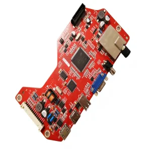
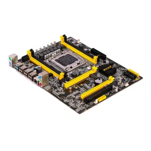
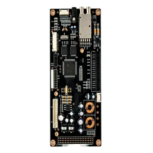
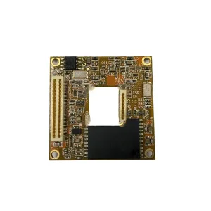
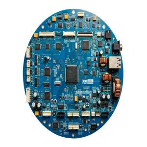
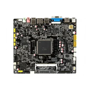
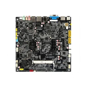
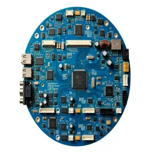
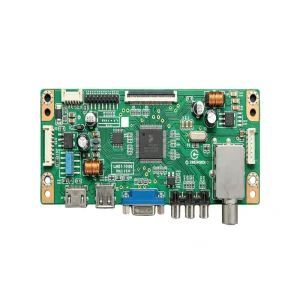
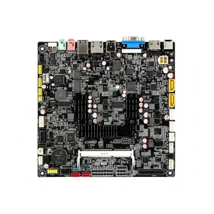
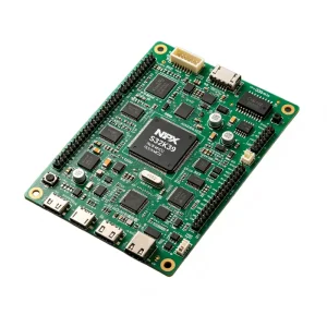
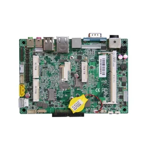
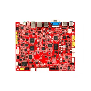
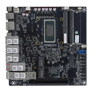
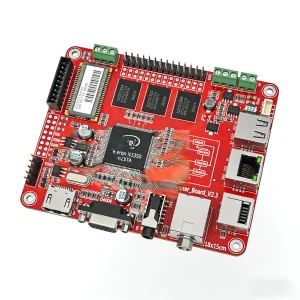
Featured commercial and industrial solutions engineered across rigorous IPC Class 2 and Class 3 electronic assembly standards.
Bridging local onshore regulatory engineering with hyper-scaled turnkey manufacturing hubs.
USA domestic electronics manufacturing operates under strict regulatory mandates including ITAR, EAR, FDA cGMP, and FCC certifications. Onshore facilities deliver unmatched rapid New Product Introduction (NPI) loops, localized hardware-in-the-loop validation, and immediate engineering alignment within North American time zones.
While USA factories excel at specialized pilot programs, volume commercialization demands deep component supply chains. Shenzhen's electronics ecosystem offers immediate access to passive and active components via direct manufacturer relationships, eradicating multi-week distribution lead times and compressing BOM costs by 30% to 55%.
Elite Fortune 500 hardware teams leverage a "Dual-Shore" manufacturing framework. Rapid prototyping, early firmware flashes, and security validations occur domestically, while mature mass volume runs migrate effortlessly to Shenzhen factories under unified IATF 16949 and ISO 13485 certifications without quality degradation.
Evaluating total cost of ownership (TCO), delivery velocity, and operational compliance profiles.
| Evaluation Parameter | OEM USA Domestic Factory | China (Shenzhen STHL) Turnkey Facility | Dual-Shore Strategic Synthesis |
|---|---|---|---|
| NPI & Quick-Turn Iterations | 24 to 72 Hours (Direct local handoff) | 3 to 5 Days (Air Express logistics) | Rapid proof-of-concept in USA; Scale in China |
| Regulatory & Defense (ITAR) | Full ITAR/DoD clearance capability | Commercial, ISO 13485, IATF 16949 | Mission-critical domestic; Non-sensitive globally |
| Component Procurement & Lead Time | Dependent on catalog distributors (Digi-Key/Mouser) | Direct Tier-1 factory networks (500k+ BOM lines) | BOM scrubbing & second-sourcing optimization |
| Scale Production Unit Economics | High labor & tooling overhead | Maximized yield, automated SMT, low labor index | 30%–50% Total Cost of Ownership reduction |
| Custom Box Build & Tooling | High-cost localized subcontracting | In-house injection tooling, metal stamping & packing | End-to-end turnkey assembly and direct DDP shipping |
Tailored manufacturing standards addressing extreme operational environments and tight compliance thresholds.
Adhering to strict IATF 16949 standards, our PCBA setups support North American electric vehicle charging infrastructure, battery management systems (BMS), and onboard telematics. Implementing automated 3D SPI, inline AOI, and high-temp potting to withstand vibration and -40°C to +125°C thermal swings.
Supporting FDA-registered OEM programs through certified ISO 13485 cleanroom assembly lines. Providing device-level traceability with full barcode-serialized work orders, Class 3 PCB routing, conformal coating against bio-contaminants, and comprehensive In-Circuit and Functional Test (FCT) validation.
Powering smart grid automation, harsh-environment remote telemetry units (RTUs), and LoRaWAN gateways. High-frequency RF tuning, micro-BGA placement (0.3mm pitch), impedance matching control within ±5%, and military-grade silicone or polyurethane conformal coatings.
Core evaluation pillars ensuring supply chain resiliency, technical competence, and IP integrity.
MES-integrated tracking tied to each SMT reel, real-time reflow profiling with 10-zone nitrogen ovens, IPC-A-610 Class 3 workmanship criteria, and complete automated optical inspection (AOI) with 3D X-ray (AXI) for BGA void verification below 15%.
Multi-layered confidentiality including bilateral NDAs enforceable in USA and Chinese courts, encrypted engineering file repositories, isolated firmware flashing cells with secured hardware tokens, and strict access controls on the factory floor.
Beyond bare board assembly: comprehensive custom wire harness fabrication, functional bed-of-nails test fixture engineering, laser-marking serialization, customized clamshell packaging, and worldwide direct drop-shipping via DHL/FedEx/UPS.
Dedicated engineering teams performing comprehensive BOM scrubbings prior to production. Identifying single-source bottlenecks, suggesting drop-in pin-compatible alternatives, and refining solder mask clearances to elevate production yields past 99.2%.
How artificial intelligence, advanced packaging, and automation redefine electronics manufacturing.
Next-generation SMT lines deploy neural networks for real-time solder paste inspection (SPI) analysis. By learning microscopic defect patterns, machine vision algorithms continuously modulate stencil wiper frequencies and squeegee pressure, achieving near-zero solder bridging on ultra-fine 01005 component footprints.
With wearables and edge AI devices demanding unprecedented compute density, PCB assembly requires complex any-layer HDI, micro-via laser drilling, and cavity-embedded passive placement. Modern automated pick-and-place lines routinely place components at ±15µm accuracy at speeds surpassing 80,000 cph.
Compliance with RoHS 3, REACH, and WEEE standards is no longer optional. Leading electronics factories adopt zero-waste closed-loop deionized water wash cycles, low-temperature soldering (LTS) alloys that curtail thermal dissipation costs by 20%, and bio-degradable ESD packaging across global shipments.
Key procurement and technical solutions addressing dual-shore supply chain management.
Enterprise hardware built with robust thermal dissipation, conformal coatings, and zero-defect SMT precision.