
Explore precision turnkey assemblies built under IATF 16949, ISO 13485, and IPC Class 3 quality protocols for critical North American industrial and commercial deployments.


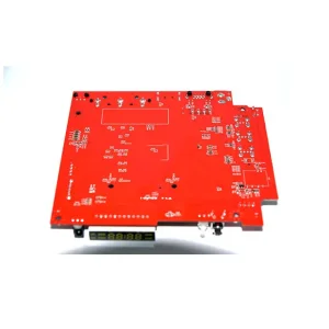
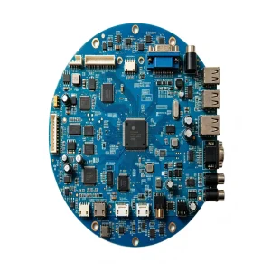
In an era defined by high component volatility, aggressive time-to-market windows, and strict regulatory hurdles, original equipment manufacturers (OEMs) across the United States are rethinking their electronics manufacturing services (EMS) architectures.
Relying exclusively on onshore USA PCB fabrication factories often imposes cost burdens that hinder global commercial competitiveness. Conversely, unvetted pure-broker offshoring exposes hardware startups and industrial pioneers to component counterfeiting, communication silos, and intellectual property vulnerabilities. The solution lies in an agile, hybrid manufacturing model.
Shenzhen STHL Electronics bridges this strategic divide. By pairing comprehensive localized USA engineering support, seamless DFM/DFA engineering consultations, and non-disclosure legal assurances with our state-of-the-art Shenzhen mega-facility, OEMs achieve rapid prototype-to-volume velocity without compromising quality, traceability, or margins.
From Silicon Valley's edge-computing micro-architectures to the Midwest's heavy industrial automation and the Sunbelt's clean-tech corridors, our customized PCB solutions power demanding environments.
Supporting North American Electric Reliability Corporation (NERC) and UL 2202 compliance standards for Level 3 DC fast-charging stations, solar inverters, and battery energy storage management systems (BEMS).
Tailored for US healthcare OEMs requiring ISO 13485 management, rigorous functional isolation, and zero failure rates in vital sign monitors, portable ultrasound units, and laboratory spectrometers.
Engineered for harsh operating parameters within automotive assembly plants, automated fulfillment centers, and water treatment analytics where thermal cycling and mechanical vibration are constant.
A pragmatic evaluation of domestic US electronics manufacturing capacity versus offshore production ecosystems, showing how procurement directors optimize capex and delivery velocity.
While federal initiatives like the US CHIPS Act emphasize domestic silicon fabrication, the domestic infrastructure for high-density, multi-layer printed circuit board bare-board manufacturing remains constrained. More than 85% of advanced multi-layer bare PCBs consumed in North America continue to rely on specialized offshore chemical plating, micro-via laser drilling, and lamination clusters.
For US-based hardware OEMs, attempting to source low-to-medium volume, 16+ layer HDI or flex-rigid assemblies solely within North America results in prohibitive 6-to-10 week lead times and 300% to 500% price premiums that reduce market competitiveness.
STHL addresses US Section 301 tariffs through intelligent supply chain structuring and turnkey delivery agreements. By managing component procurement, assembly, functional testing, and final enclosure integration (box-build) directly under one roof, the cost-per-node is drastically minimized.
Furthermore, our global logistics network facilitates Delivered Duty Paid (DDP) shipments straight to your facilities in California, Texas, Ohio, or Massachusetts. Customs documentation, classification codes (HTS), and freight forwarding are handled with complete transparency, eliminating import friction for purchasing teams.
Our engineering matrix scales alongside next-generation computing, IoT sensors, and high-voltage power electronics demands.
Substrate-Like PCB (SLP) and stacked micro-via technology down to 50µm laser micro-drills, enabling ultra-compact routing for portable wearables and avionics.
Hybrid stack-ups using Rogers (RO4350B, RO4003C), Megtron 6, and Taconic materials to sustain low insertion losses for 5G, radar, and satellite systems.
Direct copper coin bonding and Insulated Metal Substrates (IMS) engineered for extreme thermal dissipation in power supplies and automotive drivetrains.
Multi-layer flex circuits with selective adhesiveless polyimide stiffeners, delivering continuous flex-cycles for medical robotics and tight chassis integration.
| Manufacturing Parameter | Standard Commercial Spec | Advanced / Aerospace Capability | Quality Verification Standard |
|---|---|---|---|
| Layer Count | 1 to 16 Layers (Rigid FR-4) | Up to 48 Layers (Rigid / Rigid-Flex / Metal Core) | IPC-TM-650 Microsectioning |
| Min. Trace / Spacing | 3.0 mil / 3.0 mil (75µm / 75µm) | 1.8 mil / 1.8 mil (45µm / 45µm Any-Layer HDI) | AOI (Automated Optical Inspection) |
| Laser Micro-Via Diameter | 0.10 mm (4 mil) | 0.05 mm (2 mil) UV Laser Drilled | 3D X-Ray Computed Tomography |
| SMT Component Range | 0201 Passives, 0.4mm pitch BGA | 01005 Passives, 0.25mm pitch Ultra-Fine BGA / PoP | Koh Young 3D SPI & 3D AOI |
| Surface Finishes | HASL, Lead-free HASL, ENIG | ENEPIG, Immersion Silver, Hard Gold Plating (30u") | XRF Thickness Verification |
| Dielectric Materials | Standard Tg (130-140°C) FR-4 | High-Tg (170-180°C), Halogen-Free, Rogers, Polyimide | DSC (Differential Scanning Calorimetry) |
Why Tier-1 electronics brands maintain assembly and procurement centers in Shenzhen: hyper-condensed supply cluster dynamics that cannot be duplicated elsewhere.
With direct accounts and strategic alliances across distributors (DigiKey, Mouser, Arrow, Avnet) and verified Asian tier-1 manufacturers, hard-to-find passives, active microcontrollers, and specialized sensors are acquired within hours, not weeks.
Quick-turn engineering changes (ECOs) are executed in real time. Our on-site tooling workshops can modify stainless steel laser stencils, re-mill custom SMT carrier pallets, and re-profile multi-zone reflow ovens within hours of design revision approval.
New Product Introduction (NPI) teams move functional test boards from design sign-off to loaded prototypes in as little as 48 to 72 hours. Once validated, mass production scales to tens of thousands of assemblies weekly without supply interruptions.
Eliminating manufacturing flaws before they reach field operations through automated screening, thermal profiling, and electrical certification.
Statistical measurement of paste height, area, volume, and bridge offset immediately following high-precision screen printing, preventing up to 70% of potential soldering defects.
Tolerance: < 0.5µm resolutionMulti-camera top and angled optical scanning checking component presence, polarity, tombstoning, billboarding, and solder meniscus conformity across all SMD placements.
Dual-side inline inspectionNon-destructive inspection penetrating BGA, QFN, and bottom-terminated pads to calculate exact solder void percentages, bridging, and barrel fill compliance for IPC Class 3.
Void ratio guaranteed < 15%All assemblies conform strictly to IPC-A-610 Class 2 & Class 3 standards, supported by UL 94V-0 flame retardance, RoHS 3 (EU Directive 2015/863), and REACH compliance statements. Our facilities hold active certified management systems under ISO 9001:2015, ISO 13485:2016 (Medical Devices), IATF 16949:2016 (Automotive Electronics), and ISO 14001:2015 (Environmental Sustainability).
Practical, direct engineering insights addressing lead times, intellectual property protection, tariffs, and functional qualification.
We assign dedicated technical account managers and field-application engineers who overlap directly with US Eastern (EST) and Pacific (PST) business hours. Rapid engineering change reviews and quoting turnarounds typically happen within 12 to 24 hours.
We execute legally binding bilateral Non-Disclosure Agreements (NDAs) prior to receiving design files. IC programming occurs in isolated offline networks, and production firmware is cleared from test fixtures post-batch under strict digital rights protocols.
Yes. STHL manages end-to-end logistics with premier air and sea carriers (DHL, FedEx, UPS, Expeditors). We handle all import documentation, customs clearance fees, and US customs duty classifications, delivering directly to your warehouse docks.
During initial DFM/BOM scrubbing, our procurement team identifies at-risk components (NRND/EOL) and proposes Form-Fit-Function (FFF) pin-compatible second-source alternatives with full manufacturer trace documentation for engineering sign-off.
Yes. We routinely build customized in-circuit test (ICT) and functional test (FCT) jigs based on your engineering specifications. Test coverage includes power sequencing, RF RSSI calibration, CAN-bus telemetry, and real-time microcontroller programming.
To deliver a complete bare PCB and turnkey assembly quotation, we require: RS-274X or ODB++ Gerber files, an Excel BOM complete with manufacturer part numbers (MPN), Pick-and-Place centroid (XY) coordinates, and special testing instructions.
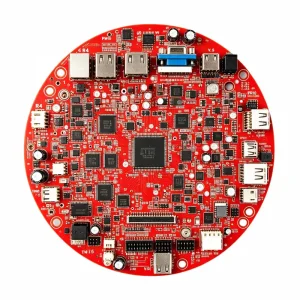
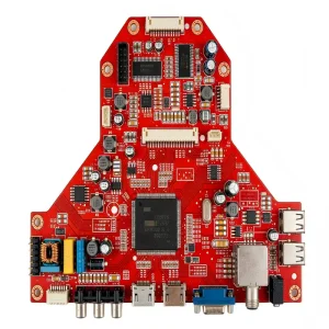
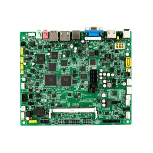
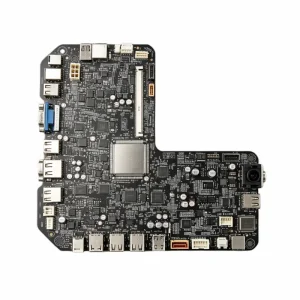
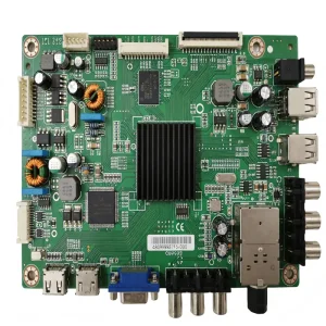
Certified assemblies deployed across demanding industrial controls, imaging infrastructure, commercial power arrays, and high-frequency RF systems.
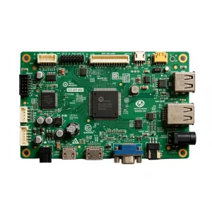
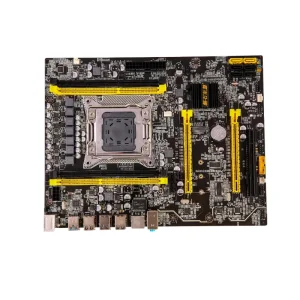

Submit your Gerber, BOM, and assembly schematics today under full NDA. Our senior engineering group returns a comprehensive DFM/DFA analysis, cost-down proposal, and turnkey fabrication timeline within 24 hours.