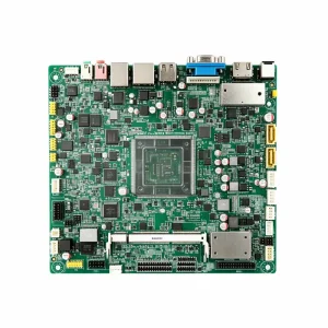
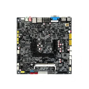
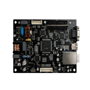
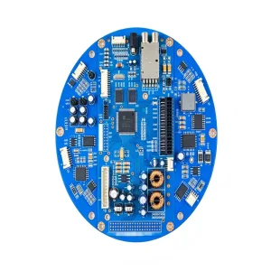
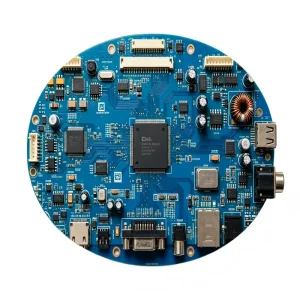
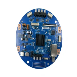
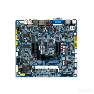
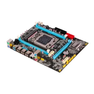
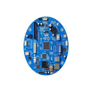
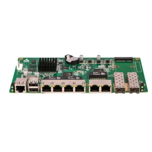
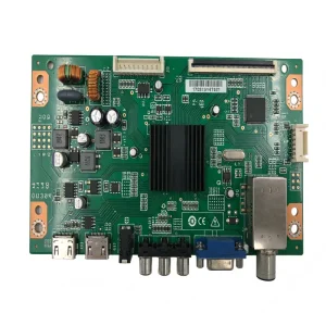
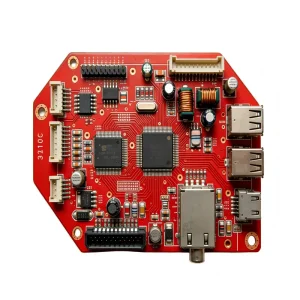
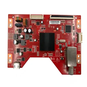
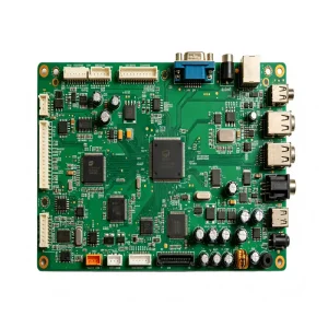
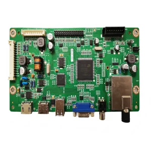
High-reliability SMT/THT boards engineered for mission-critical industrial, power, telecommunication, and avionics deployments.
In today's volatile supply ecosystem, global hardware leaders require an EMS partner capable of mitigating component obsolescence, eliminating design liabilities, and sustaining elastic volume scalability.
Global OEMs cannot afford downstream field recalls. Our adherence to IPC-A-610 Class 2 and Class 3 standards alongside strict automotive IATF 16949 process discipline ensures continuous multi-stage AOI, 3D SPI, and inline X-ray inspection (AXI) for BGA packages down to 0.3mm pitch.
Over 70% of manufacturing defects originate at the design level. Our 50+ engineers execute thorough Design for Manufacturability (DFM), Design for Testing (DFT), and Design for Assembly (DFA) audits, identifying thermal relief discrepancies, component spacing issues, and early lifecycle end-of-life (EOL) risks prior to copper etching.
Engineering innovation demands swift prototype iteration without punitive minimum order quantities. We bridge the gap from single-board engineering validation (EVT) through design validation (DVT) to high-volume commercial ramp-up (PVT) utilizing the exact same calibrated SMT production cells.
Harnessing the world's most concentrated electronics industrial cluster for unmatched procurement velocity, cost optimization, and localized component depth.
Situated in Bao'an, Shenzhen, our facility connects directly to over 100 franchised semiconductor distributors and passive component manufacturers, slashing standard lead times for critical passives, ICs, and substrates by up to 60% compared to Western assembly counterparts.
Seamless vertical integration allows instant fabrication of multi-layer standard FR-4, high-Tg materials, Roger RF high-frequency laminates, HDI microvia structures, flexible PCBs, and rigid-flex configurations with precise impedance profiling within ultra-short turnaround cycles.
Our component engineering team actively maintains a proprietary database of vetted pin-compatible second-source alternatives. When market disruptions cause allocations, we deliver functional equivalent replacements that protect schedules without sacrificing electrical fidelity.
Consolidated procurement, automated high-speed SMT mounters (0.015mm placement accuracy), automated selective soldering, and streamlined logistics result in direct bill-of-materials and labor cost savings of 25% to 40% for global technology enterprises.
Bridging Chinese manufacturing agility with Western standards of compliance, data protection, and transparent ERP/MES operational visibility.
Hardware intellectual property security is non-negotiable. We implement enterprise-grade data isolation protocols, air-gapped programming environments, and execute legally binding non-disclosure agreements prior to receiving any Gerber files, schematics, or bill of materials.
Every PCBA batch produced is strictly qualified against environmental standards including RoHS 3 (EU 2015/863), REACH (EC 1907/2006), and Conflict Minerals reporting templates (CMRT), guaranteeing frictionless market access across the European Union and North America.
Every printed circuit board is assigned a unique laser-etched 2D DataMatrix code. Our cloud-integrated Manufacturing Execution System (MES) records solder paste batch numbers, reflow thermal profiles, SMT component reel IDs, and functional test logs for up to 10 years.
Audited engineering parameters reflecting STHL's operational capacity across our 7 automated SMT lines and testing workstations.
| Parameter / Capability | Engineering Specification (Standard Production) | High-Precision / Advanced Limits |
|---|---|---|
| PCB Substrate Materials | FR-4 (Tg 130–170°C), Aluminum Core, Copper Substrates | Rogers, Megtron 6, Polyimide Flex, Ceramic, Rigid-Flex |
| Layer Count Range | 1 to 24 Layers | Up to 48 Layers (HDI any-layer via technology) |
| Min. SMD Component Size | 0201 Imperial (0.6mm × 0.3mm) | 01005 Imperial (0.4mm × 0.2mm) micro-chip placement |
| Fine Pitch & BGA Mounting | BGA Pitch 0.4mm, QFN/QFP Pitch 0.35mm | BGA Pitch down to 0.3mm with inline 3D X-Ray inspection |
| Placement Accuracy | ±0.035mm (Chips / Passives) | ±0.015mm for Ultra-fine Pitch QFP/BGA ICs |
| Soldering Technologies | Lead-Free Reflow (10-Zone Nitrogen), Wave Soldering | Selective Soldering, Vacuum Vapor-Phase Soldering |
| Testing Methodologies | Offline/Inline 3D SPI, Inline AOI, Visual Inspection | Flying Probe, ICT (In-Circuit), Functional Testing (FCT), 3D AXI |
| Conformal Coating & Potting | Manual Spray & Dip (Acrylic, Silicone) | Automated Selective Robotic Coating (Polyurethane, Epoxy, Parylene) |
Adapting to macro shifts in artificial intelligence computing, edge power density, and sustainable manufacturing practices.
Accelerating demand for edge-AI processing requires PCBA designs with dense multi-gigabit differential signaling, ultra-low insertion losses, and specialized thermal architectures. We incorporate heavy copper layers, metal thermal cores, and embedded component substrates to manage intense heat flux in AI inference cards.
Leveraging industrial IoT and predictive algorithms across our SMT stencil printers and pick-and-place lines allows real-time feedback loops. Solder paste volume variations dynamically correct stencil printer alignment, boosting First-Pass Yield (FPY) toward six-sigma operational thresholds.
With environmental criteria reshaping consumer and enterprise contracts worldwide, STHL pioneers low-temperature soldering (LTS) pastes, recyclable laminate substrates, water-soluble flux cleaning stations, and halogen-free board construction certified under ISO 14001 sustainability governance.
In-depth responses clarifying lead times, engineering handover requirements, test coverage, and IP compliance protocols.
To deliver an exhaustive engineering and commercial quotation within 24–48 hours, we require: (1) RS-274X or ODB++ Gerber files, (2) Comprehensive Bill of Materials (BOM) including Manufacturer Part Numbers (MPN), approved second sources, quantities, and reference designators, (3) Pick-and-Place Centroid file (X-Y data), (4) Assembly mechanical drawings, and (5) Specific testing/programming instructions.
STHL maintains a closed-loop supplier management system. All electronic components are procured strictly from original component manufacturers (OCM) or authorized Tier-1 global distributors (Arrow, Avnet, Digi-Key, Mouser). For legacy or discontinued parts requiring open-market procurement, incoming lots undergo decapsulation, microscopic solderability verification, X-ray leadframe inspection, and acetone surface testing.
For quick-turn prototype builds (with components in stock or standard availability), our turnaround is 3 to 7 working days post-engineering sign-off. High-volume turnkey production runs typically require 3 to 5 weeks, depending on semiconductor procurement cycles and custom PCB fabrication parameters. Safety stock and buffer inventory programs are readily available for established contract accounts.
Yes. Our in-house test engineering department routinely develops custom functional testing fixtures (bed-of-nails or pneumatic clamping systems) integrated with oscilloscopes, digital multimeters, spectrum analyzers, and automated test scripts. We provide automated firmware flashing and cryptographic key injection with secure serial logging directly into our MES database.
STHL provides complete vertical integration through our two dedicated box-build lines. Beyond PCBA manufacturing, we assemble custom wire harnesses, perform ultrasonic welding, inject adhesives, mount CNC or injection-molded enclosures, apply silicon conformal coating, pack finished retail accessories, and dispatch fully drop-tested units directly to worldwide regional hubs.
Our operations are formally certified by third-party international registrars under IATF 16949 (Automotive Quality Standard), ISO 13485 (Medical Devices Quality Management System), ISO 9001 (Quality Systems), and ISO 14001 (Environmental Management). Audits, work instructions, calibration logs, and ESD prevention frameworks are systematically updated under these standards.
Proven assembly architectures spanning medical radiography, hazardous industrial equipment, communications, and consumer platforms.