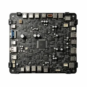
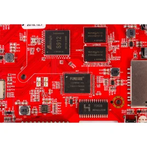
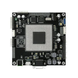
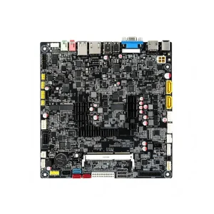
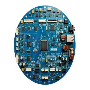
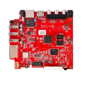
Explore initial-run functional assemblies engineered for high-frequency, telemetry, safety, and mission-critical consumer electronics.
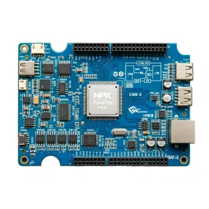
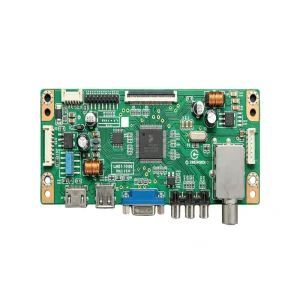
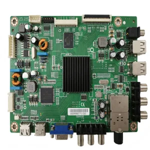
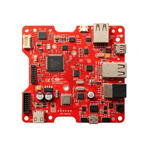
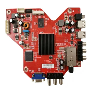
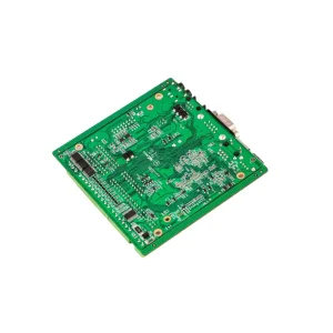
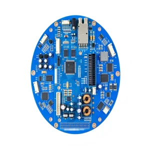

Bridging the chasm between electronic design automation (EDA) and volume mass production through zero-defect engineering.
In modern electronic product realization, the rapid validation of PCB prototypes is no longer a mere checkpoint—it is the deterministic factor in reducing Time-to-Market (TTM). Hardware engineering teams face shrinking commercialization windows where an undetected signal integrity flaw, trace thermal throttling, or component footprint mismatch can delay launch schedules by quarters and inflate capital expenditures.
The convergence of artificial intelligence, high-compute mobile architectures, and high-density interconnect (HDI) substrates has rewritten the prototyping playbook. Modern prototype boards demand sub-0.35mm pitch BGA placement, any-layer microvia laser drilling, and copper-filled via-in-pad plating. Navigating these constraints during prototype runs avoids disastrous re-spins during mass rollout.
A true OEM prototype board manufacturer operates as an extension of the client's R&D lab. Through Design for Manufacturability (DFM) and Design for Assembly (DFA) audits performed prior to copper etching, engineering teams identify tombstoning risks, solder bridge hazards, copper balance issues, and insufficient solder mask clearance before costly bare-board fabrication begins.
Why leading global industrial manufacturers, Fortune 500 tech leaders, and agile IoT start-ups anchor prototype builds in Shenzhen.
Situated within the Greater Bay Area electronics industrial cluster, Shenzhen manufacturers leverage immediate, physical proximity to the Huaqiangbei global component distribution hub and authorized tier-1 franchised distributors (Arrow, Avnet, DigiKey, Mouser). This dense spatial concentration eliminates the international logistics transit lag, allowing immediate procurement of passive reels, precision ICs, sensors, and specialty connectors within hours.
Unlike Western prototyping bureaus that batch prototype orders over multiple business days, Shenzhen's advanced facilities utilize dynamic SMT scheduling with high-speed Yamaha and Fuji pick-and-place systems. Quick feeder changeover carts, intelligent optical stencil printers, and vacuum-assisted reflow ovens run 24/7. This operational elasticity transforms a standard two-week turnaround into an expedited 48-to-72-hour delivery window.
When an OEM's prototype proof-of-concept validates successfully, moving from prototype to 100,000-unit mass production is fraught with friction if the prototyping house lacks industrial manufacturing muscle. A certified Chinese OEM/EMS provider offers complete end-to-end integration: the exact same SMT engineering teams that fine-tuned the stencil apertures for prototypes manage the automated high-volume production lines.
Demonstrated manufacturing competence spanning clinical healthcare, RF avionics, clean energy, and industrial control.
Medical PCBA prototyping operates under stringent life-critical parameters governed by ISO 13485 standards. Prototype designs for ECG monitoring devices, patient telemetry carts, and blood analyzers demand near-zero electrical noise floors. Analog frontend trace isolation, patient leakage barrier compliance (IEC 60601-1), clean room conformal coating, and strict component lot traceability prevent interference in biopotential acquisition circuits.
Navigational electronics and aerospace communication modules—such as VOR receivers and tactical modems—require extreme phase linearity, controlled dielectric constants (Dk), and minimal loss tangents (Df). Prototyping these RF boards mandates hybrid layer stack-ups that laminate high-frequency hydrocarbon/ceramic Rogers substrates onto economical FR-4 structural cores with immersion silver or ENIG surface finishes.
Solar inverters, high-efficiency modular rectifiers, and industrial open-frame power supplies introduce thermal and dielectric challenges. Prototyping in this domain requires heavy copper tracking (3 oz to 6 oz), embedded copper busbars, and thick ceramic heat dissipation planes to withstand galvanic transients and sustained high-voltage currents without thermal runaway or trace delamination.
From industrial exhaust gas spectroscopy to radiation detectors, security surveillance platforms, and municipal perimeter alarms, early-stage boards must balance low-power microcontrollers with sensitive multi-channel sensor inputs. Prototyping addresses moisture resistance, conformal dipping, analog filtering, and secure cryptographic element mounting to ensure data integrity in harsh field deployments.
Next-generation materials, miniaturization breakthroughs, and AI-driven quality assurance defining modern PCBA ecosystems.
| Technological Domain | Legacy Prototype Practices | Advanced OEM / EMS Paradigm | Impact on Enterprise Clients |
|---|---|---|---|
| Miniaturization & Pitch | 0402 passives, 0.8mm BGA, mechanical via drill | 01005 / 008004 components, 0.3mm pitch micro-BGA, laser microvias | Enables ultra-compact form factors for wearables, implants, and drone avionics. |
| Quality Verification | Manual visual inspection, periodic destructive testing | 3D SPI, 3D automated optical inspection (AOI), inline 3D AXI (X-ray) | 100% non-destructive validation of voiding ratios in hidden solder balls. |
| High-Speed Substrates | Standard FR-4 with high dielectric variance | Ultra-low loss PTFE, polyphenylene ether, embedded capacitance cores | Maintains signal integrity for 112G PAM4 transceivers and 5G/6G RF circuits. |
| Eco-Manufacturing | Traditional tin-lead, high-VOC wash chemistry | RoHS 3 / REACH compliance, zero-halogen core, bio-resin substrates | Guarantees seamless regulatory market entry into the EU, UK, and North America. |
| Digital MES Integration | Paper routing sheets, siloed departmental logs | Lot-level 2D QR trace, real-time pick-and-place nozzle telemetry | Full forensic audit trails down to individual solder reel and operator shifts. |
A structured, E-E-A-T aligned qualification framework for hardware directors, supply chain managers, and procurement leads.
Enterprise procurement teams must verify that the contract manufacturer operates under accredited ISO 9001 (Quality Management), ISO 13485 (Medical Devices), and IATF 16949 (Automotive) standards. Crucially, ask whether the factory enforces Manufacturing Execution System (MES) barcodes on prototype runs, tracking components back to original batch certificates of analysis.
Prototypes represent the culmination of proprietary corporate R&D. An authoritative OEM partner signs robust, bilateral Non-Disclosure Agreements (NDAs) prior to receiving Gerber, ODB++, or BOM data. Factory networks must maintain isolated CAD/CAM servers, internal physical security controls, and encrypted offline programming stations for proprietary firmware.
The electronic supply chain remains susceptible to counterfeit components and obsolete microcontrollers. Sourcing criteria should insist upon authorized procurement channels with full traceability to original component manufacturers (OCM). Prototyping partners must provide proactive BOM health checks—flagging End-of-Life (EOL) or Not Recommended for New Design (NRND) parts.
A supplier that outsources stencil fabrication, surface finishes, or flying probe testing introduces unnecessary communication overhead. In-house laser stencil cutting, multi-frequency impedance modeling software (Polar SI9000), dedicated first-article testing stations, and custom ICT/FCT fixture construction denote top-tier manufacturing mastery.
Detailed engineering and procurement insights addressing tolerances, turnarounds, testing coverage, and production scale.
High-reliability PCBA designs spanning power management, communications infrastructure, and precision sensing.