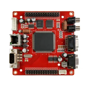
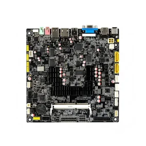
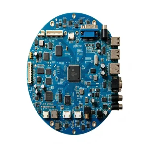
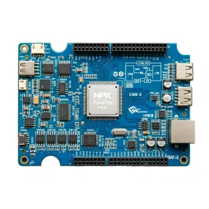
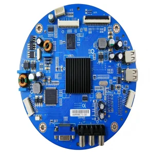
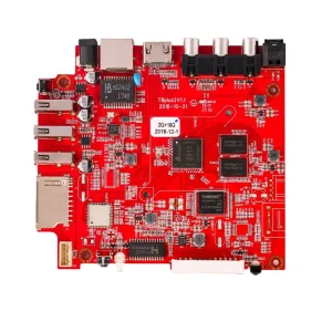
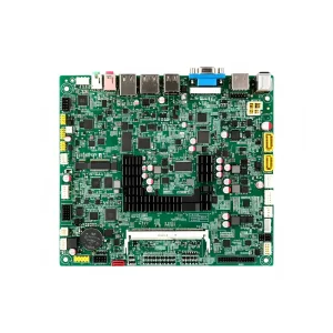
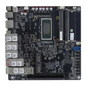
Explore our turnkey surface mount assemblies engineered for mission-critical automotive telematics, battery charging systems, life-science medical pumps, and enterprise IoT devices.
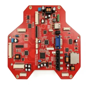
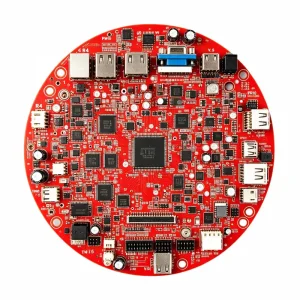

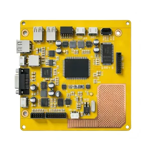
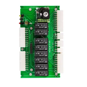
A strategic overview for global VP of Procurement, Hardware Engineering Directors, and Supply Chain Officers navigating geopolitical risk, miniaturization demands, and tier-one yield metrics.
The contemporary electronics manufacturing ecosystem has reached a critical inflection point. Hardware original equipment manufacturers (OEMs) no longer evaluate Surface Mount Technology (SMT) suppliers solely based on component placement speeds (CPH - components per hour) or standard labor arbitrage. Driven by dense computational demands in edge computing, electric vehicle (EV) powertrains, and wearable biomedical monitors, modern SMT processes require unprecedented geometric precision, absolute lot-traceability, and zero-defect quality thresholds.
The convergence of High-Density Interconnect (HDI) boards, ultra-fine-pitch Ball Grid Arrays (BGAs) down to 0.3mm ball pitch, and micro-passive packaging (01005 and 008004 chip formats) has transformed SMT assembly into a multi-variable physical-chemical science. Manufacturing defect budgets have shifted from Parts Per Million (PPM) to single-digit Parts Per Billion (PPB), mandating automated closed-loop feedback systems spanning automated optical solder paste inspection (SPI), multi-axis surface mount mounters, multi-zone nitrogen reflow profiles, and 3D automated X-ray inspection (AXI).
Strategic Procurement Insight: The true Total Cost of Ownership (TCO) in PCBA sourcing is governed not by raw board quotation rates, but by Early Life Failure Rates (ELFR), field warranty liabilities, and component lead-time mitigation through deep tier-one authorized distribution networks.
Procuring microcontrollers, power management ICs (PMICs), and passive arrays across fluctuating lead cycles demands aggressive supply chain architecture. Shenzhen STHL Electronics operates a comprehensive multi-tier sourcing framework interconnected with authorized global franchises (Digi-Key, Mouser, Arrow, Avnet) and verified direct-from-fab pipelines. Every incoming component reel undergoes strict AS6081-aligned counterfeit prevention inspections, including decapsulation sampling, solderability verification, and X-ray fluorescence (XRF) elemental material analysis before advancing to warehouse buffer storage.
Verifiable operational capabilities powering mission-critical PCBA delivery across 90+ countries worldwide.
A granular technical walk-through of the six precision manufacturing stages executed under MES (Manufacturing Execution System) tracking in our Shenzhen facility.
Prior to tooling fabrication, Gerber, ODB++, and centroid data undergo deep DFM (Design for Manufacturability) audits. Engineers simulate thermal balance, copper distribution, solder mask clearances, and component keep-out zones to eliminate reflow tombstoning risks.
Fully automated DEK printers apply lead-free SAC305 / SACX solder alloys through electro-polished, nanocoated laser stencils. Downstream 3D Solder Paste Inspection (SPI) calculates deposit height, volume, coplanarity, and bridge alerts in real time.
Dual-lane, multi-gantry Panasonic and Yamaha chip mounters place 01005 passive chips and complex QFN, WLCSP, and fine-pitch BGAs with placement repeatability within ±15 microns. Laser optical alignment verifies lead integrity before tactile contact.
Multi-zone convection reflow ovens maintain oxygen-depleted nitrogen environments (<500 ppm O2) to optimize wetting curves, mitigate void formation under large thermal pads, and ensure balanced liquidus dwell times (TAL) across disparate thermal masses.
Inline Koh Young 3D AOI identifies cold solder joints, skew, missing chips, and polarity errors using shadow-free moiré fringe projection. High-resolution 3D Automated X-ray Inspection (AXI) checks hidden BGA balls for void ratios (<15%) and bridging.
Assemblies advance to selective wave/robotic soldering, automated robotic silicone or polyurethane conformal coating, IC firmware flashing, In-Circuit Testing (ICT), functional testing (FCT), and final electromechanical box-build assembly.
Benchmark STHL's baseline production line capabilities against your upcoming hardware design requirements.
| Process Parameter | Standard Capability | Advanced / High-Density Capability | Verification Equipment / Method |
|---|---|---|---|
| Min. Passive Size | 0201 (0.6mm × 0.3mm) | 01005 (0.4mm × 0.2mm) / 008004 | High-Magnification Optical & 3D SPI |
| Min. IC Pitch (QFP / BGA) | 0.4mm pitch (QFP), 0.5mm ball pitch (BGA) | 0.3mm fine pitch / Ultra-CSP | Laser Guided Mounters + 3D Micro-Focus X-Ray |
| Placement Accuracy | ±0.035mm (3 sigma) | ±0.015mm (3 sigma) | Cpk Statistical Process Control > 1.67 |
| PCB Dimensions (Max / Min) | Min: 50mm × 50mm / Max: 510mm × 460mm | Max length up to 1200mm (LED strips) | Dual-Track Automated Conveyor Lines |
| Board Thickness Range | 0.4mm – 4.0mm | 0.2mm (Flex/Rigid-Flex) to 6.0mm | Pneumatic Clamping & Vacuum Support Fixtures |
| Reflow Soldering Environment | Standard Air Forced Convection | Nitrogen (N2) Chamber Atmosphere (<500ppm O2) | KIC Real-time Profiler + Oxygen Analyzer |
| Testing Methodologies | Visual Inspection + In-Circuit Test (ICT) | Flying Probe + 3D AOI + AXI + Custom FCT Rigs | LabVIEW Custom Rigs, High-Voltage Dielectric Test |
Tailored manufacturing programs, specialized cleanroom protocols, and sector-specific testing workflows.
IATF 16949 certified production lines supporting Advanced Driver Assistance Systems (ADAS), Telematics Box (T-Box) units, Battery Management Systems (BMS), and vehicle lighting with strict PPAP Level 3 documentation.
ISO 13485 compliant SMT for patient monitors, infusion pumps, biological analyzers, and diagnostic hardware. Built with total lot-to-carton traceability, bio-burden controls, and IPC Class 3 soldering standards.
Heavy copper PCB assemblies, industrial motor drivers, high-reliability inverter power boards, and smart grid meters requiring conformal coating, thermal potting, and 100% full-load burn-in chamber stress screening.
Multi-layer RF/Microwave mixed-signal assemblies, smart home environmental sensors, LPWAN modules, and 5G telecommunication infrastructure boards characterized for controlled impedance and RF performance.
As semiconductor lithography scales below 3nm, packaging densities force SMT lines into semi-cleanroom hybrid environments. STHL is proactively modernizing its smart factory layout through three fundamental engineering roadmaps:
1. Autonomous Closed-Loop Smart Feedback: Integrating our Koh Young 3D SPI systems directly with screen printers via industrial IoT M2M communication protocols. When solder paste volume deviates by ±5%, the SPI autonomously recalibrates printer squeegee pressure and stencil wipe cycles without human operator latency.
2. Low-Temperature Soldering (LTS) & Carbon Neutrality: Implementing advanced Bismuth-Tin (Bi-Sn) based alloys that lower peak reflow temperatures from 245°C down to 175°C. This reduction lowers thermal stress on delicate MEMS sensors while decreasing overall factory energy consumption by up to 28% in alignment with global Scope 1 and Scope 2 GHG targets.
3. Advanced Rigid-Flex & Embedded Component Substrates: Integrating passive resistors and capacitors directly into inner PCB prepregs, freeing up surface area on high-density edge-computing modules and eliminating parasitic inductance at high microwave frequencies.
Enterprise safeguards that ensure design security, strict NDA enforcement, and multi-jurisdictional compliance.
Automotive defect prevention and zero-defect quality systems.
Medical device manufacturing with absolute batch traceability.
Quality management and verified environmental stewardship.
Air-gapped firmware servers and legally binding bilateral NDAs.
Schedule a live video walk-through or request a formal DFM & BOM quotation analysis from our senior engineering team within 24 hours.
Clear, unvarnished engineering answers covering DFM thresholds, BGA rework policies, solder void tolerances, and production lead times.
Explore our specialized surface mount assemblies engineered for smart home gateways, tele-health infrastructure, automotive electronics, and environmental telemetry.