Turnkey IATF 16949-grade electronic manufacturing for autonomous vehicle platforms, EV powertrains, and connected ADAS architectures engineered for Bay Area tech pioneers.
Send Inquiry NowIntegrated micro-electronics designed to survive rigorous thermal, mechanical, and electrical automotive stress profiles.
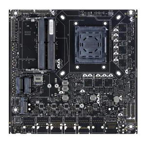
San Francisco Mission-Critical Harsh-Environment PCBA
High-Quality Aerospace PCB Assembly: Engineering Reliability for Extreme Environments Manufacturer, Service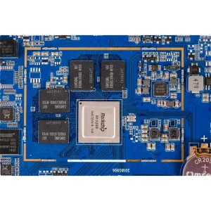
Automotive In-Cabin High-Density Processing Engine
High-Quality Laptop PCB Assembly Service, Factory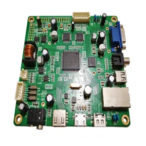
San Francisco Next-Gen AR Heads-Up Display (HUD) PCBA
High-Quality Heads-Up Display (HUD) PCBA Assembly--STHL Manufacturer, Factories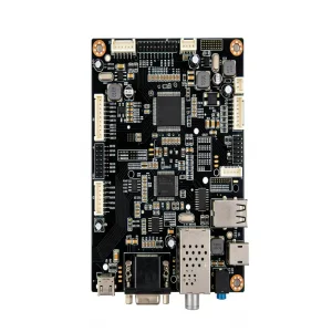
Automotive In-Cabin Driver Biometrics & Diagnostic Sensor
High-Quality Smart Blood Glucose Monitor PCB Assembly--STHL Manufacturers, FactoriesThe San Francisco Bay Area sits at the undisputed epicentre of algorithmic intelligence and software-defined vehicle (SDV) architectures. As autonomy shifts from R&D test fleets along the 101 corridor to commercial robotaxis and electrification infrastructure, hardware requirements demand unprecedented reliability.
Bay Area autonomous developers are rapidly phasing out distributed Electronic Control Units (ECUs) in favor of centralized High-Performance Compute (HPC) domains. Our SMT operations deploy ultra-fine-pitch 0.35mm pitch BGA placement, multi-layer HDI (up to 32 layers), and embedded micro-via architectures configured to handle multi-gigabit radar, camera, and LiDAR pipelines without signal degradation.
With major electric vehicle pioneers clustered between South San Francisco and Fremont, thermal management in high-voltage distribution has become a decisive differentiator. We assemble heavy copper circuits (up to 6 oz), ceramic-filled thermal substrates, and direct aluminum baseplates designed for 800V DC-DC converters and bidirectional onboard chargers.
Iterative engineering cycles in Mission Bay and Silicon Valley cannot afford multi-week turnaround lags. Our hybrid manufacturing pipeline combines immediate local DFM consulting with scalable high-throughput SMT lines, executing rapid NPI (New Product Introduction) cycles that transition smoothly into zero-defect mass production.
Navigating global semiconductor volatility while meeting stringent automotive environmental guidelines demands full lifecycle transparency.
Counterfeit mitigation is non-negotiable for safety-critical hardware. We enforce complete lot-level component traceability through authorized distribution networks (Arrow, Avnet, Digi-Key, Mouser), utilizing MES serialization to match every micro-resistor and automotive SoC to its original wafer lot.
Defect prevention supersedes defect detection. Our lines employ 3D Solder Paste Inspection (SPI), high-resolution 3D Automated Optical Inspection (AOI), and multi-angle inline Automated X-ray Inspection (AXI) to verify non-destructive voiding thresholds below 10% on safety-critical QFNs and ball grid arrays.
Automotive hardware must maintain profitability at scale. Our engineering desk conducts comprehensive BOM health checks, pinpointing sole-sourced microcontrollers, proposing AEC-Q qualified pin-compatible alternates, and optimizing PCB panel utilization to drive raw fabrication yields past 99.4%.
Every board leaving our facility meets strict automotive compliance mandates, calibrated to survive severe vibrational shock, thermal cycling, and aggressive chemical exposure.
Certified quality management specifically structured for automotive product realization, incorporating APQP, PPAP Level 3, and FMEA protocols.
Full lifecycle functional safety process execution to eliminate systematic faults in ADAS hardware, braking modules, and autonomous steering circuits.
Strict assembly criteria for dedicated service electronic products where continuous operation is critical and downtime cannot be tolerated.
100% active and passive component screening for AEC-Q100 (ICs), AEC-Q101 (Discretes), and AEC-Q200 (Passives) qualification profiles.
From dynamic urban test tracks in Downtown San Francisco to autonomous trucking routes traversing Northern California, our PCBA solutions power critical mobility systems.
Supporting frequency ranges beyond 77 GHz. Our PTFE, Rogers, and high-frequency hybrid multilayer laminates deliver minimal insertion loss and dielectric stability, ensuring autonomous fleets process real-time point clouds under dense fog, precipitation, and complex urban clutter.
High-voltage isolation arrays (exceeding 2,500V DC) integrated with precision thermal sensor chains. We engineer slave and master battery control architectures featuring conformal coating and encapsulation to prevent dendritic short-circuits caused by condensation or chemical exposure.
Delivering uninterrupted 5G-NR cellular, DSRC, and GPS/GNSS synchronization across smart mobility fleets. Integrated RF shielding enclosures, automated selective soldering, and robust transient voltage suppression prevent signal dropout and electromagnetic interference (EMI).
Anticipating the technological disruptions that will reshape San Francisco's smart infrastructure, our assembly processes are continuously upgrading to match next-generation architectures.
Embedding GaN fast-switching transistors directly into heavy-copper internal layers, drastically cutting thermal resistance and weight in power inverters.
Transitioning from pure copper high-speed traces to silicon photonics boards to satisfy the 100+ Gbps bandwidth required by L4/L5 full self-driving processors.
Merging capacitive touch, dynamic LED backlighting, and flex circuitry directly into structural composite vehicle interiors, reducing assembly wire harness mass by up to 40%.
Essential technical insights for engineering managers, procurement executives, and system architects qualifying automotive assembly partners.
From initial Gerber review and Bill of Materials optimization to zero-defect IATF 16949-grade electronics manufacturing, our engineering team is ready to support your hardware roadmap.
Send Inquiry NowDiscover our turnkey circuit assembly capabilities spanning automotive telematics, intelligent sensors, and edge-connected systems.
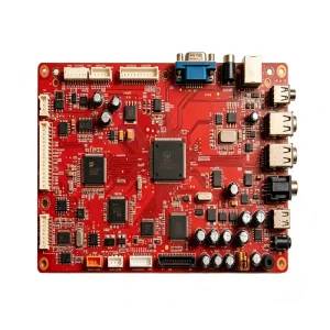
San Francisco In-Vehicle GPS & Navigation System Assembly
OEM Car Navigation Systems PCBA Assembly--STHL Manufacturer, Manufacturers
Automotive Diagnostic Handheld Optical Barcode PCBA
China Medical Barcode Scanner PCB Assembly--STHL Manufacturer, Service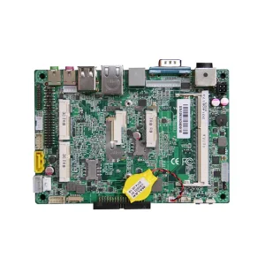
Electric Vehicle Solar-Roof & Energy Monitor Controller
High-Quality Photovoltaic Module Monitor PCB Assembly Manufacturers, Factories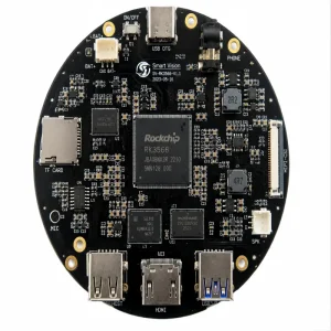
Automotive Ethernet & Industrial Gateway Interface Board
OEM Power over Ethernet Injector (PoE Injector) PCB Assembly--STHL Manufacturers, Service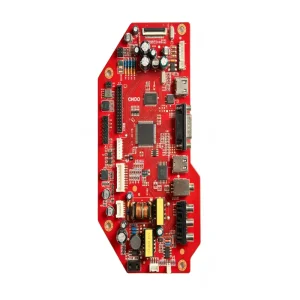
San Francisco Multi-Zone Cabin Thermal Management PCBA
High-Quality Smart Thermostat PCBA Assembly--STHL Manufacturer, Factory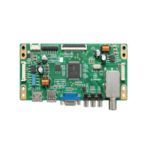
Automotive Road Obstacle & Inductive Proximity Detector
OEM Metal Detector PCB Assembly--STHL Manufacturer, Manufacturers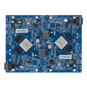
High-Efficiency Power Distribution Board for Smart Mobility
China Consumer Electronics PCBA Application: Powering the Devices of Tomorrow Manufacturer, Service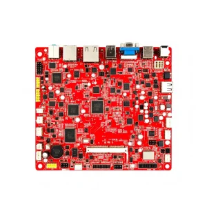
San Francisco Autonomous Vehicle IMU & Dynamic Motion Sensor
High-Quality Motion Sensor PCBA Assembly--STHL Manufacturer, Factories